CY7C056V-20AI Просмотр технического описания (PDF) - Cypress Semiconductor
Номер в каталоге
Компоненты Описание
производитель
CY7C056V-20AI Datasheet PDF : 22 Pages
| |||
PRELIMINARY
CY7C056V
CY7C057V
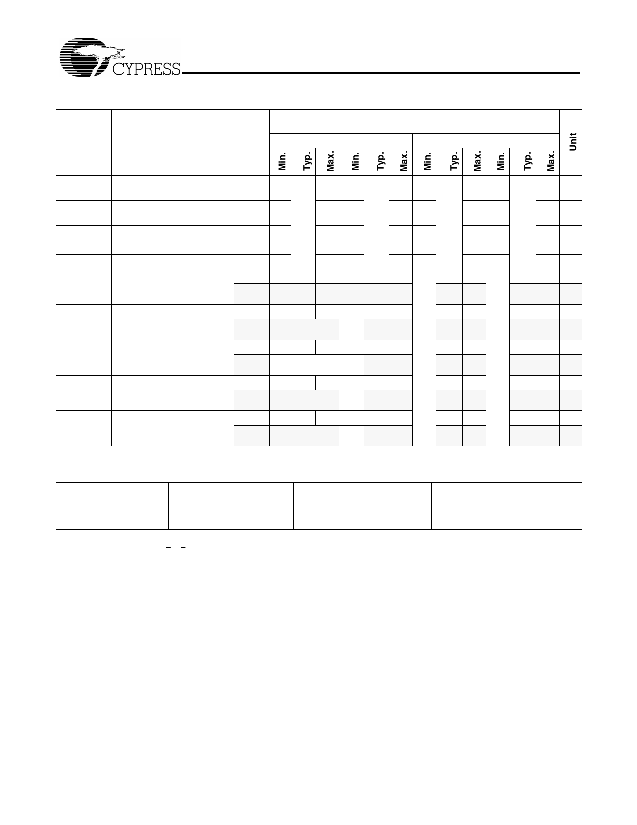
Electrical Characteristics Over the Operating Range [7, 8]
CY7C056V
CY7C057V
-10
-12
-15
-20
Parameter
Description
VOH
Output HIGH Voltage
(VDD = Min., IOH = –4.0 mA)
2.4
2.4
2.4
2.4
V
VOL
Output LOW Voltage
(VDD = Min., IOL = +4.0 mA)
0.4
0.4
0.4
0.4 V
VIH
Input HIGH Voltage
2.0
2.0
2.0
2.0
V
VIL
Input LOW Voltage
0.8
0.8
0.8
0.8 V
IOZ
Output Leakage Current
-10
10 –10
10 –10
10 –10
10 µA
ICC
Operating Current (VDD = Com’l.
260 410
250 385
240 360
230 340 mA
Max., IOUT = 0 mA) Outputs Indust.
Disabled
265 385
mA
ISB1
Standby Current (Both Ports Com’l.
60 80
55 75
50 70
45 65 mA
TTL Level and Deselected)
f = fMAX
Indust.
65 95
mA
ISB2
Standby Current (One Port Com’l.
185 250
180 240
175 230
165 210 mA
TTL Level and Deselected) Indust.
f = fMAX
190 255
mA
ISB3
Standby Current (Both Ports Com’l.
0.01 1
0.01 1
0.01 1
0.01 1 mA
CMOS Level and Deselect- Indust.
ed) f =0
0.01 1
mA
ISB4
Standby Current (One Port
CMOS Level and Deselect-
ed) f = fMAX[9]
Shaded areas contain advance information.
Com’l.
Indust.
170 220
160 210
155 200
170 215
145 180 mA
mA
Capacitance[10]
Parameter
Description
Test Conditions
Max.
Unit
CIN
COUT
Input Capacitance
Output Capacitance
TA = 25°C, f = 1 MHz,
VDD = 3.3V
10
pF
10
pF
Notes:
7. Cross Levels are VDD – 0.2V< VZ<0.2V.
8. Deselection for a port occurs if CE0 is HIGH or if CE1 is LOW.
9. fMAX = 1/tRC = All inputs cycling at f = 1/tRC (except Output Enable). f = 0 means no address or control lines change. This applies only to inputs at CMOS level
standby ISB3.
10. Tested initially and after any design or process changes that may affect these parameters.
6
Share Link: 