WS1403 Просмотр технического описания (PDF) - Avago Technologies
Номер в каталоге
Компоненты Описание
производитель
WS1403 Datasheet PDF : 15 Pages
| |||
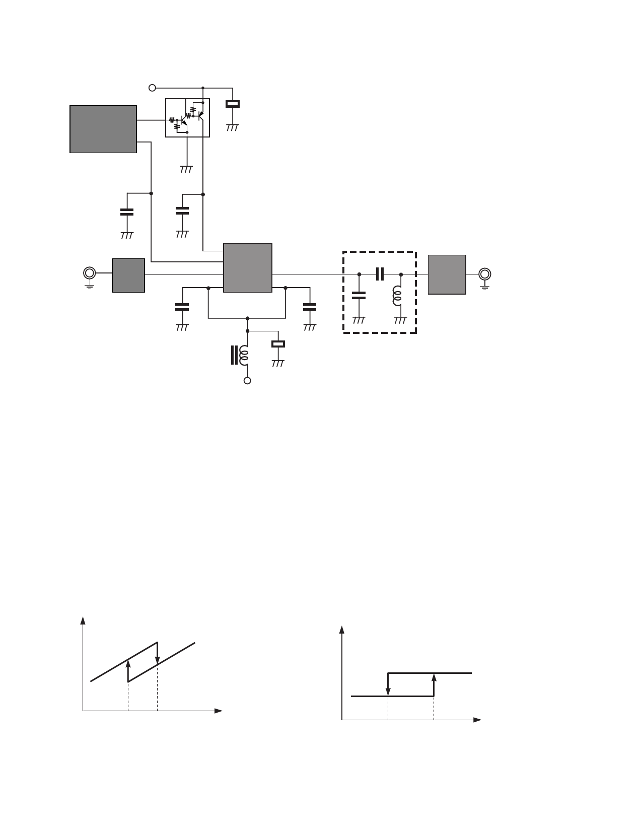
Peripheral Circuit in Handset
+2.85 V
C8
MSM PA_ON
PA_RO
C2
C1
RF In
TX
FILTER
C3
WS1403
Vref
Vcont
GND
GND
RF IN RF OUT
Vcc1
Vcc2
Output Matching Circuit
C6
RF Out
Duplexer
C7
L1
C4
C5
VBATT
Figure 10. Peripheral circuit
Notes:
• Recommended voltage for Vref is 2.85 V.
• Place C1 near to Vref pin.
• Place C3 and C4 close to pin 4 (Vcc1) and pin 5 (Vcc2). These capacitors can affect the RF performance.
• Use 50 W transmission line between PAM and Duplexer and make it as short as possible to reduce conduction loss.
• π-type circuit topology is good to use for matching circuit between PA and Duplexer.
Calibration
Calibration procedure is shown in Figure 11. Two
calibration tables, high mode and low mode respectively,
are required for Cool PAM, which is due to gain difference
in each mode. For continuous output power at the mode
change points, the input power should be adjusted
according to gain step during the mode change.
TX_AGC
Offset Value (Difference between Rising Point and Falling
Point)
Offset value, which is the difference between the rising
point (output power where PA mode changes from low
mode to high mode) and falling point (output power
where PA mode changes from high mode to low mode),
should be adopted to prevent system oscillation. 3 to 5
dB is recommended for hysteresis.
GAIN
Low Mode
High Mode
Falling Rising
Min. PWR
Pout
Max. PWR
Figure 11. Calibration procedure
Low Mode
High Mode
Pout
Falling
Rising
Figure 12. Setting of offset between rising and falling power
Share Link: 