VRS1000 Просмотр технического описания (PDF) - Unspecified
Номер в каталоге
Компоненты Описание
производитель
VRS1000 Datasheet PDF : 47 Pages
| |||
VRS1000
VERSA
Datasheet Rev 1.6
IAP Chip Erase Function
The IAP chip erase function will erase the entire flash
memory content with the exception of the ISP boot
program area. Running this function will also
automatically unprotect the flash memory.
IAP Chip Protect Function
The chip protect function when executed makes the
chip Flash memory content to read as 00h when an
attempt is made to read it.
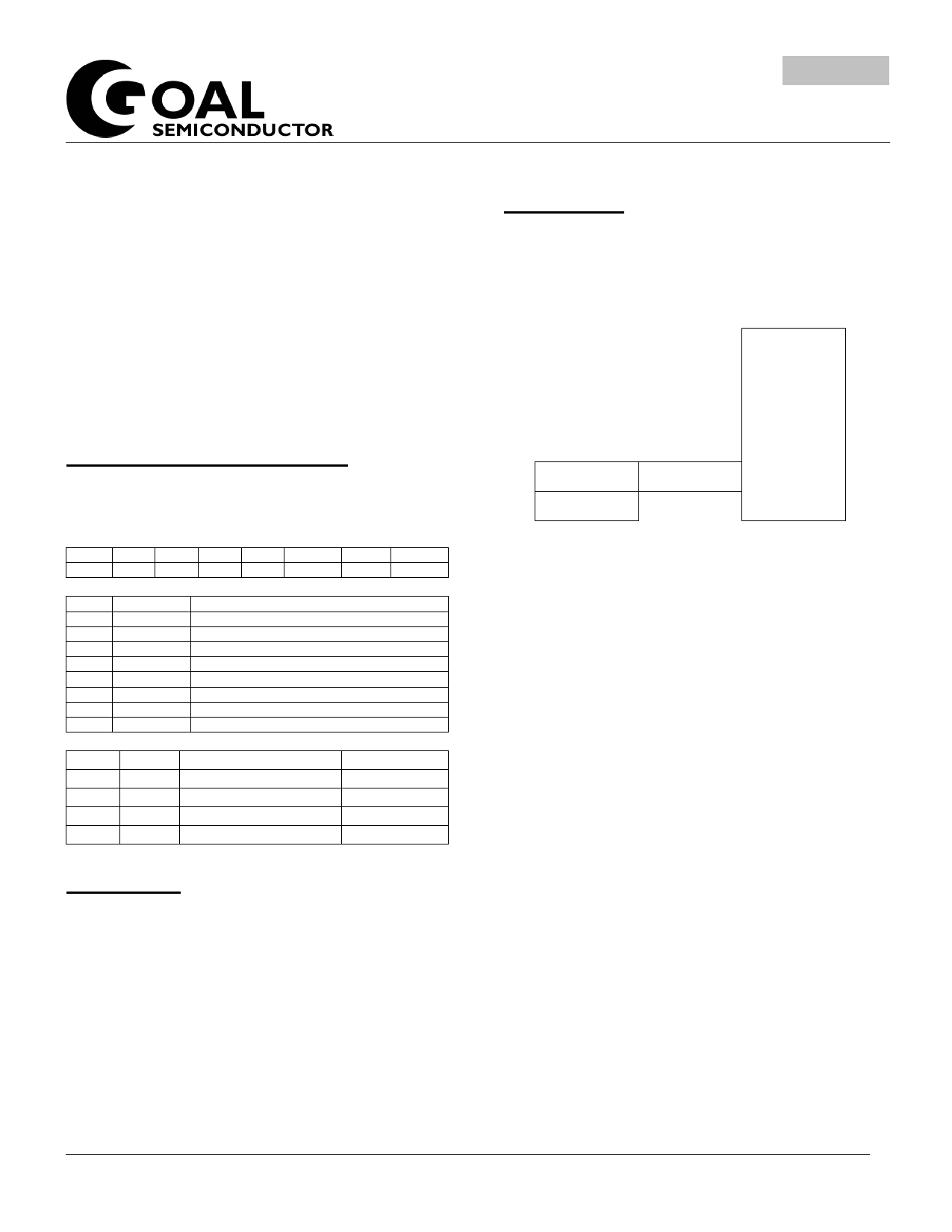
Program Status Word Register
The register below contains the program state flags.
These flags may be read or written to by the user.
TABLE 11: PROGRAM STATUS WORD REGISTER (PSW) - SFR DOH
7
6
5
4
3
2
1
0
CY AC F0 RS1 RS0 OV
-
P
Bit Mnemonic Description
7
CY
Carry Bit
6
AC
Auxiliary Carry Bit from bit 3 to 4.
5
F0
User definer flag
4
RS1
R0-R7 Registers bank select bit 0
3
RS0
R0-R7 Registers bank select bit 1
2
OV
Overflow flag
1
-
-
0
P
Parity flag
RS1 RS0
0
0
0
1
1
0
1
1
Active Bank
0
1
2
3
Address
00h-07h
08h-0Fh
10h-17h
18-1Fh
Data Pointer
The VRS1000 has one 16-bit data pointer. The DPTR
is accessed through two SFR addresses: DPL located
at address 82h and DPH located at address 83h.
Data Memory
The VRS1000 has 1K of on-chip RAM: 256 bytes are
configured like the internal memory structure of a
standard 80C52, while the remaining 768 bytes can be
accessed using external memory addressing (MOVX).
FIGURE 6: VRS1000 DATA MEMORY
02FF
Expanded 768 bytes
(Can by accessed by
direct external addressing
mode, using the MOVX
instruction)
FF
Upper 128 bytes
FF
SF R
(Can only be accessed in
(Can only be accessed in direct
80
indirect addressing mode)
addressing mode)
7F
Lower 128 bytes
80
(Can be accessed in indirect and
direct addressing mode)
00
(XRAME=1)
0000
By default after reset, the expanded RAM area is
disabled. It can be enabled by setting the XRAME bit
of the SYSCON register located at address BFh in the
SFR.
Lower 128 bytes (00h to 7Fh, Bank 0 & Bank 1)
The lower 128 bytes of data memory (from 00h to 7Fh)
can be summarized in the following points:
o Address range 00h to 7Fh can be accessed in
direct and indirect addressing modes.
o Address range 00h to 1Fh includes R0-R7
registers area.
o Address range 20h to 2Fh is bit addressable.
o Address range 30h to 7Fh is not bit
addressable and can be used as general-
purpose storage.
Upper 128 bytes (80h to FFh, Bank 2 & Bank 3)
The upper 128 bytes of the data memory ranging from
80h to FFh can be accessed using indirect addressing
or by using the bank mapping in direct addressing
mode.
1134 Ste Catherine Street West, Suite 900, Montreal, Quebec, Canada H3B 1H4 Tel: (514) 871-2447 http://www.goalsemi.com
9
Share Link: 