TDA3615J Просмотр технического описания (PDF) - Philips Electronics
Номер в каталоге
Компоненты Описание
производитель
TDA3615J Datasheet PDF : 18 Pages
| |||
Philips Semiconductors
Multiple voltage regulator
Product specification
TDA3615J
LIMITING VALUES
In accordance with the Absolute Maximum Rating System (IEC 60134).
SYMBOL
PARAMETER
Vbat/I(ig)
supply voltage
operating
jump start
load dump protection
Vrp
Ptot
Tstg
Tamb
Tj
reverse polarity voltage
total power dissipation
storage temperature
ambient temperature
junction temperature
CONDITIONS
MIN.
regulators on
−
t ≤ 10 minutes
−
t ≤ 50 ms; tr ≥ 2.5 ms −
non-operating
−
Tamb = 25 °C
−
non-operating
−55
operating
−40
operating
−40
MAX.
18
30
50
−18
62.5
+150
+85
+150
UNIT
V
V
V
V
W
°C
°C
°C
THERMAL CHARACTERISTICS
SYMBOL
PARAMETER
CONDITIONS
Rth(j-c)
Rth(j-a)
thermal resistance from junction to case
thermal resistance from junction to ambient in free air
VALUE
2
40
UNIT
K/W
K/W
QUALITY SPECIFICATION
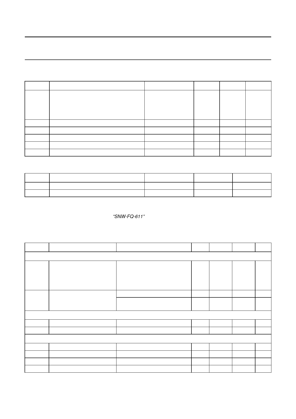
Quality specification is in accordance with “SNW-FQ-611”.
CHARACTERISTICS
Vbat = VI(ig) = 14.4 V; Tamb = 25 °C; see Fig.4; unless otherwise specified.
SYMBOL
PARAMETER
CONDITIONS
Supply
Vbat/I(ig)
Iq
supply voltage
operating
jump start
load dump protection
quiescent supply current
regulators on
t ≤ 10 minutes
t ≤ 50 ms; tr ≥ 2.5 ms
Vbat = 14.4 V; VI(ig) < 1 V; note 1
Vbat = VI(ig) = 14.4 V;
selector inputs 0,0,0; note 1
Reset buffer
Isink(L)
Rpu(int)
LOW-level sink current
internal pull-up resistance
Selector control inputs
VIL
LOW-level input voltage
VIH
HIGH-level input voltage
IIH
HIGH-level input current
IIL
LOW-level input current
VIH > 2 V
VIL < 0.8 V
MIN. TYP.
11
14.4
−
−
−
−
−
110
−
125
2
15
3.7 4.7
−0.5 −
2.0 −
−
−
−1.0 −
MAX. UNIT
18
V
30
V
50
V
250
µA
−
µA
−
mA
5.7
kΩ
+0.8
V
−
V
1.0
mA
−
mA
2004 Jan 12
7
Share Link: 