TDA3615J Просмотр технического описания (PDF) - Philips Electronics
Номер в каталоге
Компоненты Описание
производитель
TDA3615J Datasheet PDF : 18 Pages
| |||
Philips Semiconductors
Multiple voltage regulator
Product specification
TDA3615J
FUNCTIONAL DESCRIPTION
The TDA3615J is a multiple voltage regulator intended to
supply a microprocessor (e.g. in car radio applications).
Because of low-voltage operation of the application,
a low-voltage drop regulator is used in the TDA3615J.
Regulator 1 (5 V standby) will switch on when the supply
voltage exceeds 7.2 V for the first time and will switch off
again when the output voltage of the regulator drops below
3.5 V.
Reset is used to indicate that the regulator output voltage
is within its voltage range. This start-up feature is built-in to
secure a smooth start-up of the microprocessor at first
connection, without uncontrolled switching of the standby
regulator during the start-up sequence.
All other regulators and switches can be switched on and
off by using the three control input pins. This is only
possible when both supply voltages (Vbat and VI(ig)) are
within their voltage range. Table 1 shows all possible
states.
The filament regulator output voltage of the TDA3615J can
be adjusted with pin FILADJ.
All output pins are fully protected. The regulators are
protected against load dump and short-circuit (foldback
current protection, except the filament regulator output).
At load dump all regulator outputs will go LOW except the
5 V standby regulator output.
The antenna switch and the media switch can withstand
‘loss of ground’. This means that the ground pin is
disconnected and the switch output is connected to ground
(Vbat and VI(ig) are normally connected to the right pin).
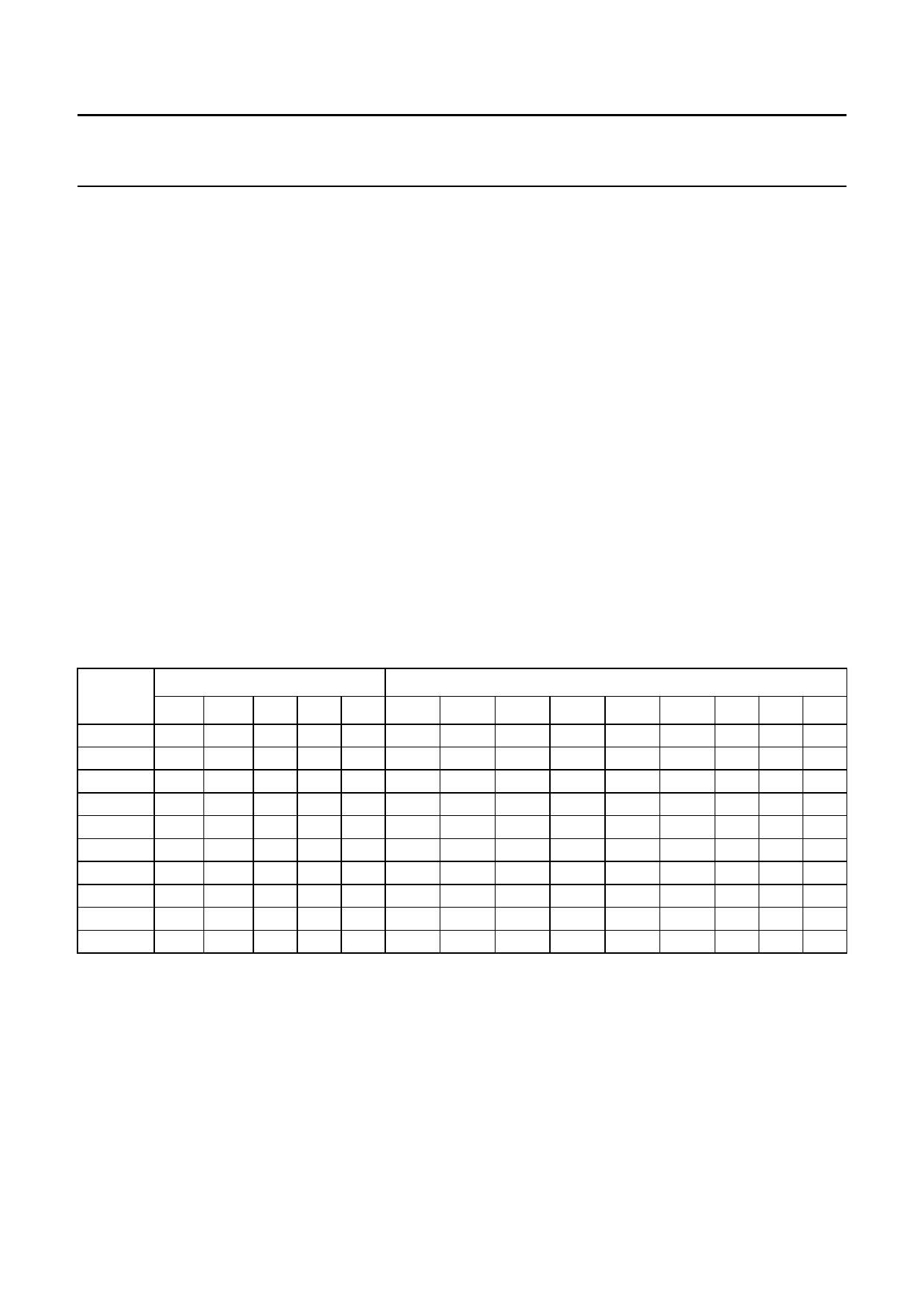
Selector settings
Table 1 Possible states of outputs depending on inputs
STATE
1
2
3
4
5
6
7
8
9
10
INPUTS
OUTPUTS
Vbat Vl(ig) EN1 EN2 EN3 REG1 REG2 REG3 REG4 REG5 REG6 SW1 SW2 SW3
0
X(1) X(1) X(1) X(1)
0
0
0
0
0
0
000
1
0
X(1) X(1) X(1)
1
0
0
0
0
0
000
1
1
000
1
0
0
0
0
0
000
1
1
001
1
1
1
1
0
1
101
1
1
010
1
1
1
1
1
0
101
1
1
011
1
1
1
0
0
0
011
1
1
100
1
1
1
0
0
0
001
1
1
101
1
1
1
1
0
1
111
1
1
110
1
1
1
1
1
0
111
1
1
111
1
1
1
1
0
0
111
Note
1. X = don’t care.
2004 Jan 12
6
Share Link: 