STLC4420A Просмотр технического описания (PDF) - STMicroelectronics
Номер в каталоге
Компоненты Описание
производитель
STLC4420A Datasheet PDF : 40 Pages
| |||
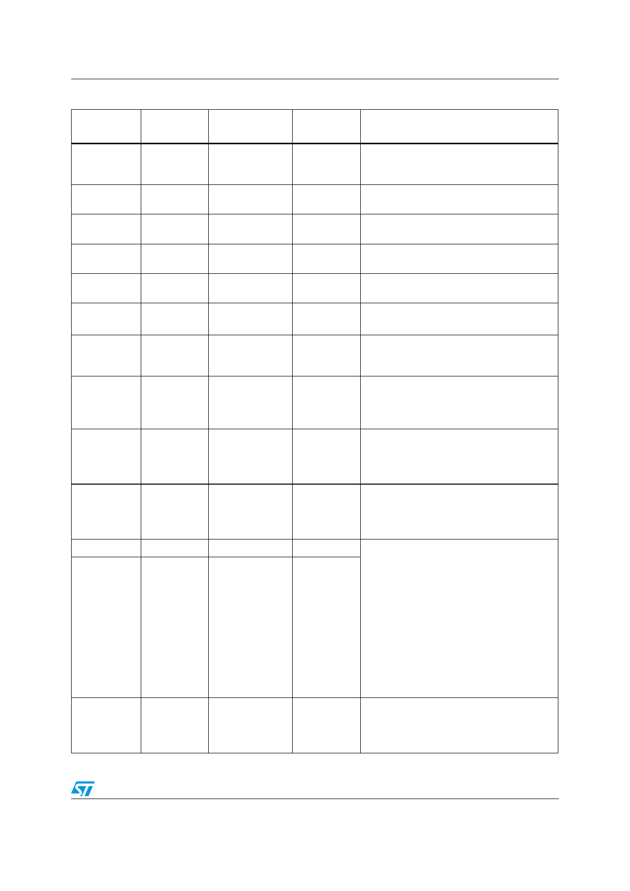
STLC4420A
Pin descriptions
Table 1. STLC4420A signal descriptions (continued)
Pin name Pin number
Type
Internal
resistor
Function
REF_CLK
N10
LF_XTAL_IN B23
SPI_CLK
B22
SPI_CSX
A20
SPI_DIN
D24
SPI_DOUT B17
FREQ
C21
RF_ACTIVE E24
STATUS
A19
TX_CONF
B19
MODE0
M5
MODE1
L6
HISPEED_
N4
BUS_SEL
Clock input
1.8 V (VIO) digital
input
1.8 V (VIO) digital
input
1.8V (VIO) digital
input
1.8 V (VIO) digital
I/O
1.8 V (VIO) digital
output
1.8 V (VIO) GPIO
(input)
1.8 V (VIO) GPIO
(input)
1.8 V (VIO) GPIO
(input)
1.8 V (VIO) GPIO
(output)
1.8 V digital input
1.8 V digital input
1.8 V digital input
Reference clock input (19.2, 26.0, 38.4 or
-
40.0 MHz). Use a 1000pF typical series
blocking capacitor.
32KHz typical sleep clock input from host.
SPI clock from host
No Pull
No Pull
No Pull
No Pull
SPI chip select from host
SPI data input for 4-wire modes. In 3-wire
modes, this is the data input/output signal.
SPI data output for 4-wire modes only.
In SDIO mode pin = DAT0.
Firmware controlled GPIO typically
implementing Bluetooth coexistence FREQ
input function. Assigned to ARM MAC GP2-6.
Firmware controlled GPIO typically
implementing Bluetooth coexistence
RF_ACTIVE input function. Assigned to ARM
MAC GP2-5.
Firmware controlled GPIO typically
implementing Bluetooth coexistence STATUS
input function.
Assigned to ARM MAC GP2-4.
Firmware controlled GPIO typically
implementing Bluetooth coexistence
TX_CONF output function.
Assigned to ARM MAC GP2-3.
MODE strapping pins are pimarily used to
properly initialize the PLL for following
REF_CLK frequencies.
Connect appropriate pin to ground plane for a
logic 0 input or to 1.8V power plane (through
a 4kohm resistor) for a logic 1.
MODE(1:0) = 00 => 19.2 MHz
MODE(1:0) = 01 => 40 MHz default, no pull
needed
MODE(1:0) = 10 => 26 MHz
MODE(1:0) = 11 => 38.4 MHz
(Note: M5=RX0, L6=RX1)
High speed internal bus selection input.
Needs to be pulled down through 2.5K ohm to
set the proper high speed bus mode.
(Note: N4 = ANTSELTST+)
7/40
Share Link: 