ST230C Просмотр технического описания (PDF) - International Rectifier
Номер в каталоге
Компоненты Описание
производитель
ST230C Datasheet PDF : 8 Pages
| |||
ST230C..C Series
Bulletin I25162 rev. D 04/03
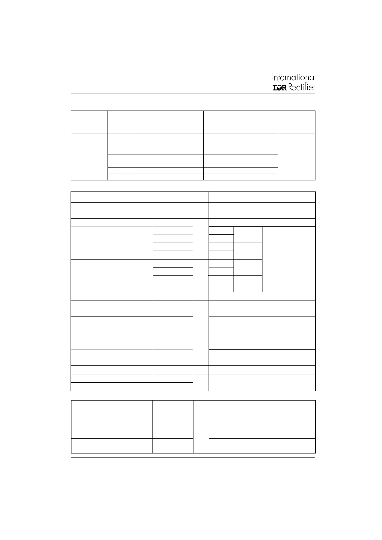
ELECTRICAL SPECIFICATIONS
Voltage Ratings
Voltage
Type number Code
VDRM/VRRM, max. repetitive
peak and off-state voltage
V
04
08
ST230C..C
12
14
16
18
20
400
800
1200
1400
1600
1800
2000
On-state Conduction
VRSM , maximum non-
repetitive peak voltage
V
500
900
1300
1500
1700
1900
2100
IDRM/IRRM max.
@ TJ = TJ max
mA
30
Parameter
ST230C..C Units Conditions
IT(AV) Max. average on-state current
@ Heatsink temperature
IT(RMS) Max. RMS on-state current
ITSM Max. peak, one-cycle
non-repetitive surge current
I2t
Maximum I2t for fusing
I2√t Maximum I2√t for fusing
VT(TO)1 Low level value of threshold
voltage
VT(TO)2 High level value of threshold
voltage
rt1
Low level value of on-state
slope resistance
rt2
High level value of on-state
slope resistance
VTM Max. on-state voltage
IH
Maximum holding current
IL
Max. (typical) latching current
Switching
410 (165)
55 (85)
780
5700
5970
4800
5000
163
148
115
105
1630
0.92
0.98
A 180° conduction, half sine wave
°C double side (single side) cooled
DC @ 25°C heatsink temperature double side cooled
t = 10ms No voltage
A t = 8.3ms reapplied
t = 10ms 100% VRRM
t = 8.3ms reapplied
Sinusoidal half wave,
KA2s
KA2√s
t = 10ms No voltage
t = 8.3ms reapplied
Initial TJ = TJ max.
t = 10ms
t = 8.3ms
100% VRRM
reapplied
t = 0.1 to 10ms, no voltage reapplied
(16.7% x π x IT(AV) < I < π x IT(AV)), TJ = TJ max.
V
(I > π x IT(AV)),TJ = TJ max.
0.88
0.81
1.69
600
1000 (300)
(16.7% x π x IT(AV) < I < π x IT(AV)), TJ = TJ max.
mΩ
(I > π x IT(AV)),TJ = TJ max.
V
Ipk= 880A, TJ = TJ max, tp = 10ms sine pulse
mA TJ = 25°C, anode supply 12V resistive load
di/dt
Parameter
Max. non-repetitive rate of rise
of turned-on current
td
Typical delay time
tq
Typical turn-off time
ST230C..C
1000
1.0
100
Units Conditions
A/µs
µs
Gate drive 20V, 20Ω, tr ≤ 1µs
TJ = TJ max, anode voltage ≤ 80% VDRM
Gate current 1A, dig/dt = 1A/µs
Vd = 0.67% VDRM, TJ = 25°C
ITM = 300A, TJ = TJ max, di/dt = 20A/µs, VR = 50V
dv/dt = 20V/µs, Gate 0V 100Ω, tp = 500µs
2
www.irf.com
Share Link: 