SST39LF200A Просмотр технического описания (PDF) - Microchip Technology
Номер в каталоге
Компоненты Описание
производитель
SST39LF200A Datasheet PDF : 37 Pages
| |||
A Microchip Technology Company
2 Mbit / 4 Mbit / 8 Mbit Multi-Purpose Flash
SST39LF200A / SST39LF400A / SST39LF800A
SST39VF200A / SST39VF400A / SST39VF800A
Data Sheet
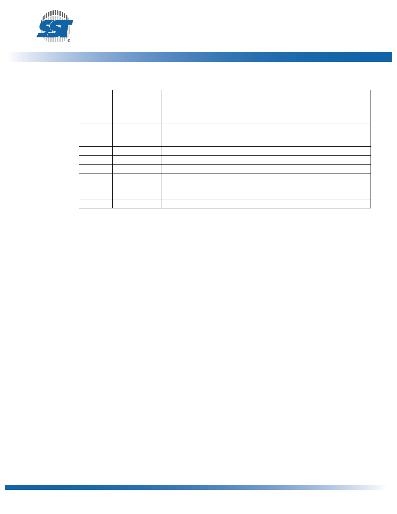
Table 1: Pin Description
Symbol Pin Name
Functions
AMS1-A0
Address Inputs
To provide memory addresses. During Sector-Erase AMS-A11 address lines will
select the sector. During Block-Erase AMS-A15 address lines will select the
block.
DQ15-DQ0 Data Input/output To output data during Read cycles and receive input data during Write cycles.
Data is internally latched during a Write cycle.
The outputs are in tri-state when OE# or CE# is high.
CE#
Chip Enable
To activate the device when CE# is low.
OE#
Output Enable To gate the data output buffers.
WE#
Write Enable
To control the Write operations.
VDD
Power Supply To provide power supply voltage: 3.0-3.6V for SST39LF200A/400A/800A
2.7-3.6V for SST39VF200A/400A/800A
VSS
Ground
NC
No Connection Unconnected pins.
1. AMS = Most significant address
AMS = A16 for SST39LF/VF200A, A17 for SST39LF/VF400A, and A18 for SST39LF/VF800A
T1.2 25001
©2011 Silicon Storage Technology, Inc.
6
DS25001A
03/11
Share Link: 