SPT9101 Просмотр технического описания (PDF) - Fairchild Semiconductor
Номер в каталоге
Компоненты Описание
производитель
SPT9101 Datasheet PDF : 8 Pages
| |||

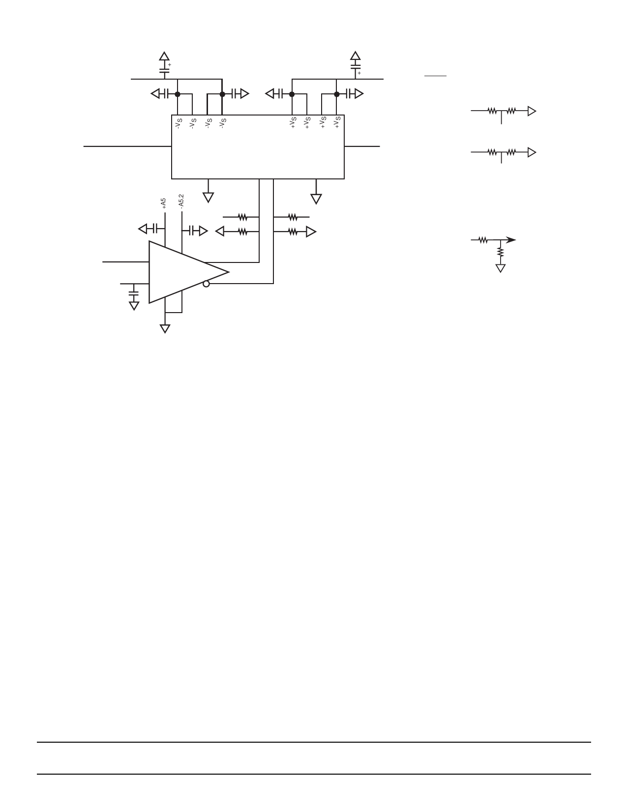
Figure 2 - Typical Interface Circuit
+
2.2 µF
-A5.2
+ 2.2 µF
+A5
12 13 17 18
4 58 9
VIN
15
VIN
SPT9101
RTN
1,2
CLK NCLK
10
11
18
VOUT
GND
6,7,16
330
-A5.2
2
220
CLK IN
X
Vt
8
3
VCC
11
IN+
VEE
SPT, HCMP96850
4
IN-
GND
LE
12
1,16
6
330
-A5.2
220
VOUT
NOTES:
1) Vt = Threshold voltage:
a) For TTL or CMOS Clock input
+A5
3k 1k
Vt
b) For ECL Clock input
-A5.2
3k 1k
Vt
2) Unless otherwise specified, all capacitors
are 0.01 or 0.1 µF, surface mount.
3) X = Termination (if required).
4) CLKIN
a) TTL/CMOS
CLKIN
R
96850
R
b) ECL: Direct Input
THEORY OF OPERATION
The SPT9101 is a monolithic 125 MSPS track and hold
amplifier built on a very high-speed complementary bipolar
process. It is pin and functionally compatible with the AD9101.
It is a two stage design with a sampler driving a hold capacitor
followed by a noninverting output buffer amplifier with gain of
4. The first stage sampler is based on a current amplifier in
noninverting gain of one configuration with inverting input
connected to the output. The hold switch is integrated into this
closed-loop first stage amplifier.
The output buffer amplifier is in a noninverting gain of 4
configuration with inverting input connected to a resistor
divider driven from the output. The noninverting input from the
hold capacitor employs input bias current cancellation which
results in excellent droop rate performance. The sampler and
amplifier stages both employ complementary current ampli-
fiers for high-speed, low-distortion performance.
TYPICAL INTERFACE CIRCUIT
BOOTSTRAP CAPACITOR
The SPT9101 does not require the bootstrap capacitor that is
required on the AD9101 between pins 3 and 19. Because
pins 3 and 19 are No Connects on the SPT9101, it will work
well in existing AD9101 sockets.
CLOCK DRIVER CIRCUIT (CLK, NCLK PINS)
Fairchild highly recommends that a differential ECL clock be
used to drive the SPT9101. Both the 10KH and 100KH family
of ECL logic can be used. The typical interface diagram,
figure 2, shows the use of a SPT HCMP96850 high-speed
comparator. The comparator has a typical propagation delay
of 2.4 ns, very low offset of 3 mV, and a minimum tracking
bandwidth of 300 MHz. The comparator shown has been set
up in a feedthrough operation mode with latch enable con-
nected to a logic high.
The threshold voltage (Vt) can be set using a resistor divider
as shown in note 1 of figure 2. The configuration shown in
note 1a is for a TTL/CMOS clock input and the configuration
shown in note 1b is for an ECL clock input. The differential
output of the comparator is directly fed to the SPT9101 clock
input. The comparator can also be driven with a sinewave
input, with the threshold voltage (Vt) adjusted to produce the
desired track/hold duty cycle ratio.
Note 4a shows the resistor divider configuration for a TTL/
CMOS clock input. If an ECL clock is used it can be directly
fed into the comparator.
OUTPUT LEVEL SHIFTING (RTN PIN)
The RTN pin is tied to the output buffer amplifier internal
feedback resistor network as shown in the block diagram.
Normally this pin is tied to ground for a 4x gain output amplifier
configuration. However, this pin may be configured in other
ways as long as certain guidelines are met.
SPT9101
5
12/30/99