SG3825CQ Просмотр технического описания (PDF) - Microsemi Corporation
Номер в каталоге
Компоненты Описание
производитель
SG3825CQ Datasheet PDF : 7 Pages
| |||
PRODUCT DATABOOK 1996/1997
SG1825C/SG2825C/SG3825C
HIGH-SPEED CURRENT-MODE PWM
NOT RECOMMENDED FOR NEW DESIGNS
A P P L I C AT I O N I N F O R M AT I O N
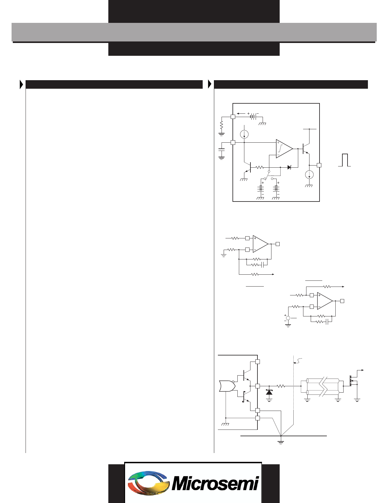
OSCILLATOR
The oscillator frequency is programmed by external timing components RT
and CT. A nominal +3.0 volts appears at the RT pin. The current flowing
through RT is mirrored internally with a 1:1 ratio. This causes an identical
current to flow out the CT pin, charging the timing capacitor and generating
a linear ramp. When the upper threshold of +2.8 volts is reached, a
discharge network reduces the ramp voltage to +1.0, where a new charge
cycle begins.
The Clock output pin is LOW (+2.3 volts) during the charge cycle, and
HIGH (+4.5 volts) during the discharge cycle. The Clock pin is driven by
an NPN emitter follower, and so can be wire-ORed. Each Clock pin can drive
a 1mA load. Since the internal current-source pulldown is approximately
400µA, the DC fan-out to other SG1825C Clock pins is at least two.
The type of capacitor selected for CT is very important. At high
frequencies, non-ideal characteristics such as effective series resistance
(ESR), effective series inductance (ESL), dielectric loss and dielectric
absorption all affect frequency accuracy and stability. RF capacitors such as
silver mica, glass, polystrene, or COG ceramics are recommended. Avoid
high-K ceramics, which work best in DC bypass applications.
ERROR AMPLIFIER
The voltage error amplifier is a true operational amplifier with low-
impedance output, and can be gain-stabilized using conventional feedback
techniques. The typical DC open-loop gain is 95dB, with a single low-
frequency pole at 100Hz.
The input connections to the error amplifier are determined by the
polarity of the power supply output voltage. For positive supplies, the
common-mode voltage is +5.1 volts and the feedback connections in Figure
A are used. With negative outputs, the common-mode voltage is half the
reference, and the feedback divider is connected between the negative
output and the +5.1 volt reference as shown in Figure B.
OUTPUT DRIVER
The output drivers are designed to provide up to 1.5 Amps peak output
current. To minimize ringing on the output waveform, which can be
destructive to both the power MOSFET and the PWM chip, the series
inductance seen by the drivers should be as low as possible.
One solution is to keep the distance between the PWM and MOSFET gate
as short as possible, and to use carbon composition series damping resistors.
A Faraday shield to intercept radiated EMI from the power transistors is
usually required with its choice.
A second approach is to place the MOSFETs some distance from the PWM
chip, and use a series-terminated transmission line to preserve drive pulse
fidelity. This will minimize noise radiated back to the sensitive analog
circuitry of the SG1825C. A Faraday shield may also be required.
If the drivers are connected to an isolation transformer, or if kickback
through CGD of the MOSFET is severe, clamp diodes may be required. 1 Amp
peak Schottky diodes will limit undershoot to less than -0.3 volts.
A P P L I C AT I O N F I G U R E S
FIGURE 5. OSCILLATOR FUNCTIONAL DIAGRAM
RT 5
IR
3V
CT 6
IC = IR
2.8V
SG1825C
+ 5.1V
400µA
1.0V
4 CLOCK
+ 4.5V
+ 2.3V
FIGURE 6. VOLTAGE AMPLIFIER CONNECTIONS
VREF
R1
R2
2
1
R3
3 VERROR
RZ
CP
R4
FIGURE A
POSITIVE
OUTPUT
VOLTAGE
VREF
R1
R2
VREF
2
FIGURE B
R4
2
1
R3
RZ
CP
NEGATIVE
OUTPUT
VOLTAGE
3 VERROR
FIGURE 7. DRIVING SHIELDED CABLE
SG1825C
13 VC
FARADAY SHIELD
24W
11
*
12 PWR GND
10 GND
50W
50W
* SCHOTTKY CLAMP MAY BE REQUIRED
Copyright © 1994
Rev. 1.3a
7
Share Link: 