NCP431A Просмотр технического описания (PDF) - ON Semiconductor
Номер в каталоге
Компоненты Описание
производитель
NCP431A Datasheet PDF : 16 Pages
| |||
NCP431A, SC431A, NCP431B, NCP432B Series
ELECTRICAL CHARACTERISTICS (TA = 25°C, unless otherwise noted.)
NCP431BC
NCP432BC
NCP431BI
NCP432BI
NCP431BV
NCP432BV
Symbol
Characteristic
Min Typ Max Min Typ Max Min Typ Max Unit
Vref
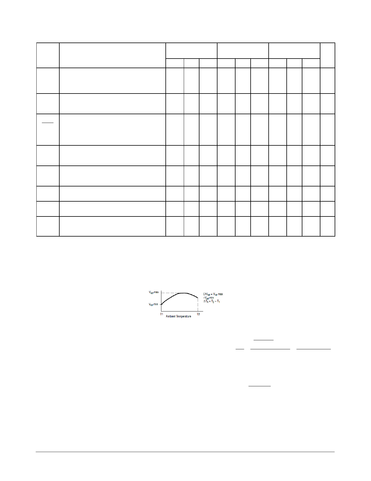
DVrefT
DVref
DVAK
Iref
DIrefT
Imin
Ioff
|ZKA|
Reference Input Voltage
VKA = Vref, IK = 1 mA
TA = 25°C
TA = Tlow to Thigh (Note 6)
Reference Input Voltage Deviation Over Tem-
perature Range (Figure 1, Notes 7, 8)
VKA= Vref, IK = 1 mA
Ratio of Change in Reference Input Voltage to
Change in Cathode to Anode Voltage
IK = 1 mA (Figure 2),
DVKA = 10 V to Vref
DVKA = 36 V to 10 V
Reference Input Current (Figure 2)
IK = 1 mA, R1 = 220 k, R2 = R
TA = −40°C to +125°C
Reference Input Current Deviation Over Tem-
perature Range (Figure 2, Note 7, 8)
IK = 1 mA, R1 = 10 k, R2 = R
Minimum Cathode Current For Regulation
VKA = Vref (Figure 1)
Off−State Cathode Current (Figure 3)
VKA = 36 V, Vref = 0 V
Dynamic Impedance (Figure 1, Note 8)
VKA = Vref, DIK = 1.0 mA to 100 mA
f v 1.0 kHz
V
2.4875 2.500 2.5125 2.4875 2.500 2.5125 2.4875 2.500 2.5125
2.4875 2.500 2.5125 2.4775 2.500 2.5125 2.4725 2.500 2.5125
−
−
−
−
−
− 5.0 10
−
1−
− 10 15 mV
−
15
− −2.00 −3.1
− −1.28 −1.9
−
81 190
− −2.00 −3.1
− −1.28 −1.9
−
81 190
mV/
V
− −2.00 −3.1
− −1.28 −1.9
nA
− 81 190
−
22 55
−
22 55
nA
− 22 55
−
40 80
−
40 80
−
40 80 mA
− 180 1000 − 180 1000 − 180 1000 nA
− 0.22 0.5
− 0.22 0.5
− 0.22 0.5 W
6. Tlow = −40°C for NCP431BI, NCP431BV, NCP432BI, NCP432BV
= 0°C for NCP431BC, NCP432BC
Thigh = 70°C for NCP431BC, NCP432BC
= 85°C for NCP431BI, NCP432BI
= 125°C for NCP431BV, NCP432BV
7. Guaranteed by design
8. The deviation parameter DVrefT is defined as the difference between the maximum and minimum values obtained over the full operating
ambient temperature range that applies.
The average temperature coefficient of the reference input voltage, Vref is defined as:
ǒ Ǔ DVref
ppm
Vref@25° C
Vref ° C +
DTA
106
+
DVref
106
DTAǒVref@25° CǓ
aVref can be positive or negative depending on whether Vref Min or Vref Max occurs at the lower ambient temperature.
Example: DVrefT = 17 mV and slope is positive
Vref = 2.5 V, DTA = 165°C (from −40°C to +125°C)
aVref
+
0.017 @ 106
165 @ 2.5
+
41.2
ppmń°
C
9. The dynamic impedance ZKA is defined as: (|ZKA| = (DVKA/DIK). When the device is programmed with two external resistors, R1 and R2,
the total dynamic impedance of the circuit is defined as: |ZKA’| [ |ZKA| (1 + (R1/R2))
http://onsemi.com
4
Share Link: 