SA8282DP1S Просмотр технического описания (PDF) - Mitel Networks
Номер в каталоге
Компоненты Описание
производитель
SA8282DP1S Datasheet PDF : 14 Pages
| |||
SA828
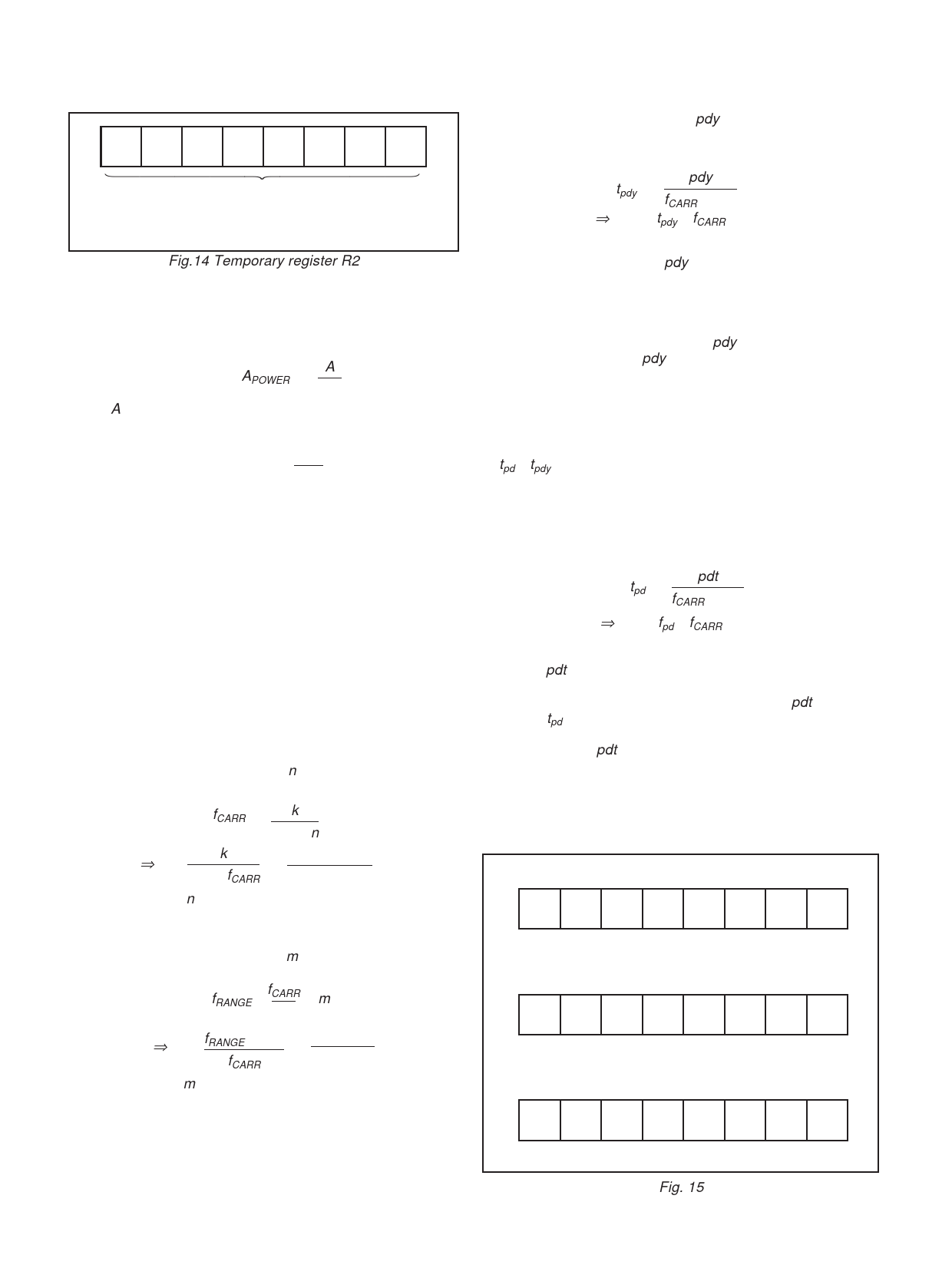
AMP7 AMP6 AMP5 AMP4 AMP3 AMP2 AMP1 AMP0
AMPLITUDE
SELECT WORD
AMP7 = MSB
AMP0 = LSB
Fig.14 Temporary register R2
Amplitude selection
The power waveform amplitude is determined by scaling
the amplitude of the waveform samples stored in the ROM by
the value of the 8-bit amplitude select word (AMP).
The percentage amplitude control is given by:
A
Power Amplitude, APOWER = 255 x 100%
where A = decimal value of AMP.
POWER-UP C0NDITIONS
All bits in both the Initialisation and Control registers power-
up in an unidentified state. Holding RST low or using the SET
TRIP input will ensure that the PWM outputs remain inactive
(i.e., low) until the device is initialised.
SA828 PROGRAMMING EXAMPLE
The following example assumes that a master clock of
12·288 MHz is used (12·288 MHz crystals are readily available).
This clock frequency will allow a maximum carrier frequency of
24 kHz and a maximum power frequency of 4 kHz.
Initialisation Register Programming Example
A power waveform range of up to 250Hz is required with a
carrier frequency of 6kHz, a pulse deletion time of 10µs and an
underlap of 5µs.
1. Setting the carrier frequency
The carrier frequency should be set first as the power
frequency, pulse deletion time and pulse delay time are all
defined relative to the carrier frequency.
We must calculate the value of n that will give the required
carrier frequency:
fCARR =
k
512 x n
⇒n=
k
= 12·288 x 106 = 4
512 x fCARR 512 x 6 x 103
From Table 4, n = 4 corresponds to a 3-bit CFS word of
010 in temporary register R1.
2. Setting the power frequency range
We must calculate the value of m that will give the required
power frequency:
fRANGE
=
fCARR x
384
m
⇒ m = fRANGE x 384 = 250 x 384
fCARR
6 x 103
= 16
From Table 5, m = 16 corresponds to a 3-bit FRS word of
100 in temporary register R1.
3. Setting the pulse delay time
As the pulse delay time affects the actual minimum pulse width
seen at the PWM outputs, it is sensible to set the pulse delay time
before the pulse deletion time, so that the effect of the pulse delay
time can be allowed for when setting the pulse deletion time.
8
We must calculate the value of pdy that will give the required
pulse delay time:
pdy
tpdy = fCARR x 512
⇒ pdy = tpdy x fCARR x 512
= 5 x 10–6 x 6 x 103 x 512 = 15·4
However, the value of pdy must be an integer. As the
purpose of the pulse delay is to prevent ‘shoot-through’ (where
both top and bottom arms of the inverter are on simultaneously),
it is sensible to round the pulse delay time up to a higher, rather
than a lower figure.
Thus, if we assign the value 16 to pdy this gives a delay time
of 5·2µs. From Table 6, pdy = 16 corresponds to a 6-bit PDY
word of 110000 in temporary register R2.
4. Setting the pulse deletion time
In setting the pulse deletion time (i.e., the minimum pulse
width) account must be taken of the pulse delay time, as the
actual minimum pulse width seen at the PWM outputs is equal
to tpd – tpdy.
Therefore, the value of the pulse deletion time must, in this
instance, be set 5·2µs longer than the minimum pulse length
required
Now,
Minimum pulse length required = 10µs
∴ tPD to be set to 10µs + 5·2µs = 15·2µs
pdt
tpd = fCARR x 512
⇒ pdt = fpd x fCARR x 512
= 15·2 x 10–6 x 6 x 103 x 512 = 46·7
Again, pdt must be an integer and so must be either rounded
up or down – the choice of which will depend on the application.
Assuming we choose in this case the value 46 for pdt, this gives
a value of tpd, of 15 µs and an actual minimum pulse width of 15
– 5·2µs = 9·8µs.
From Table 7, pdt = 46 corresponds to a value of PDT, the
7-bit word in temporary register R0 of 1010010.
The data which must be programmed into the three temporary
registers R0, R1 and R2 (for transfer into the initialisation
register) in order to achieve the parameters in the example
given, is shown in Fig. 15.
Temporary Register R0
11010010
CR PDT6 PDT5 PDT4 PDT3 PDT2 PDT1 PDT0
Temporary Register R1
1 0 0XX0 1 0
FRS2 FRS1 FRS0 X X CFS2 CFS2 CFS2
Temporary Register R2
XX1 1 0 0 0 0
X X PDY5 PDY4 PDY3 PDY2 PDY1 PDY0
Fig. 15
Share Link: 