R80C188XL-25 Просмотр технического описания (PDF) - Intel
Номер в каталоге
Компоненты Описание
производитель
R80C188XL-25 Datasheet PDF : 48 Pages
| |||
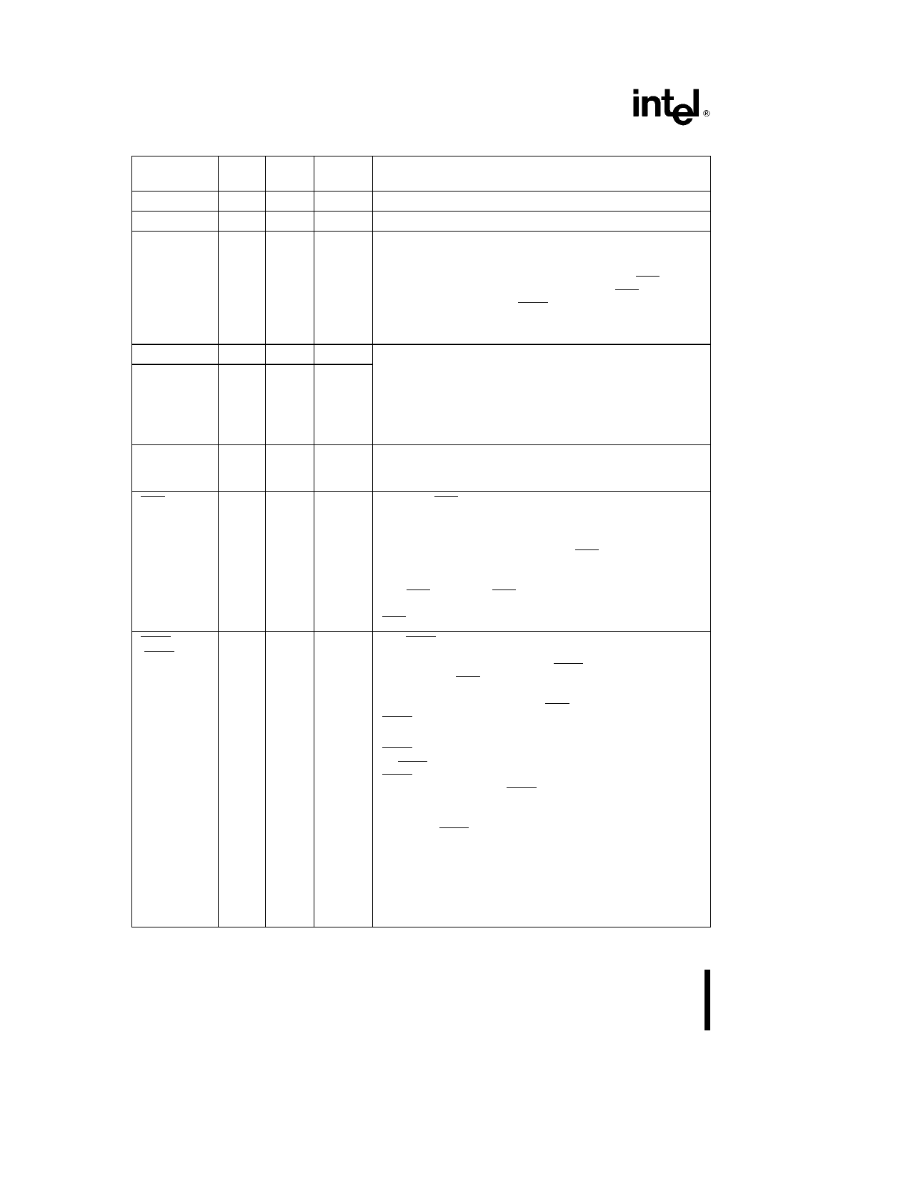
80C186XL 80C188XL
Pin
Name
VCC
VSS
RESET
X1
X2
CLKOUT
RES
TEST BUSY
(TEST)
Pin
Type
P
G
O
I
O
O
I
I
Input
Type
A(E)
A(L)
A(E)
Table 3 Pin Descriptions
Output
States
Pin Description
System Power a5 volt power supply
System Ground
H(0) RESET Output indicates that the CPU is being reset and can
R(1) be used as a system reset It is active HIGH synchronized
with the processor clock and lasts an integer number of
clock periods corresponding to the length of the RES signal
Reset goes inactive 2 clockout periods after RES goes
inactive When tied to the TEST BUSY pin RESET forces
the processor into enhanced mode RESET is not floated
during bus hold
H(Q)
R(Q)
Crystal Inputs X1 and X2 provide external connections for a
fundamental mode or third overtone parallel resonant crystal
for the internal oscillator X1 can connect to an external
clock instead of a crystal In this case minimize the
capacitance on X2 The input or oscillator frequency is
internally divided by two to generate the clock signal
(CLKOUT)
H(Q)
R(Q)
Clock Output provides the system with a 50% duty cycle
waveform All device pin timings are specified relative to
CLKOUT CLKOUT is active during reset and bus hold
An active RES causes the processor to immediately
terminate its present activity clear the internal logic and
enter a dormant state This signal may be asynchronous to
the clock The processor begins fetching instructions
approximately 6 clock cycles after RES is returned HIGH
For proper initialization VCC must be within specifications
and the clock signal must be stable for more than 4 clocks
with RES held LOW RES is internally synchronized This
input is provided with a Schmitt-trigger to facilitate power-on
RES generation via an RC network
The TEST pin is sampled during and after reset to determine
whether the processor is to enter Compatible or Enhanced
Mode Enhanced Mode requires TEST to be HIGH on the
rising edge of RES and LOW four CLKOUT cycles later Any
other combination will place the processor in Compatible
Mode During power-up active RES is required to configure
TEST BUSY as an input A weak internal pullup ensures a
HIGH state when the input is not externally driven
TEST In Compatible Mode this pin is configured to operate
as TEST This pin is examined by the WAIT instruction If the
TEST input is HIGH when WAIT execution begins instruction
execution will suspend TEST will be resampled every five
clocks until it goes LOW at which time execution will
resume If interrupts are enabled while the processor is
waiting for TEST interrupts will be serviced
BUSY (80C186XL Only) In Enhanced Mode this pin is
configured to operate as BUSY The BUSY input is used to
notify the 80C186XL of Math Coprocessor activity Floating
point instructions executing in the 80C186XL sample the
BUSY pin to determine when the Math Coprocessor is ready
to accept a new command BUSY is active HIGH
NOTE
Pin names in parentheses apply to the 80C188XL
10
Share Link: 