PFM19030 Просмотр технического описания (PDF) - Cree, Inc
Номер в каталоге
Компоненты Описание
производитель
PFM19030 Datasheet PDF : 15 Pages
| |||
PFM19030
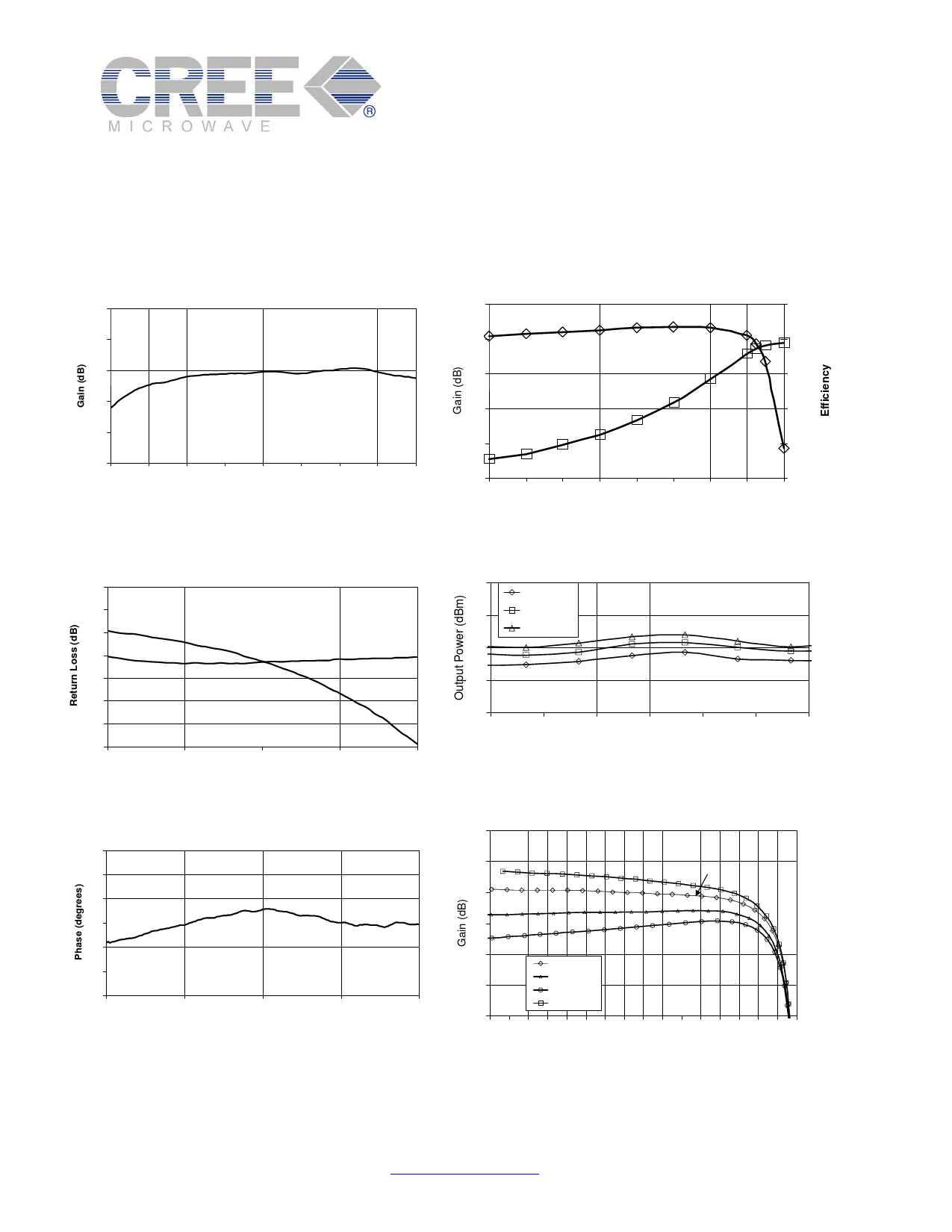
Typical Module Performance
T=+25 °C, unless otherwise noted. Data is for module in a test fixture with external matching elements. See following
page for test fixture details.
Typical Small-Signal Gain vs. Frequency
31
30
Gain & Efficiency vs. Output Power
Pulsed Measurement, Vdc=+27V, F=1960 MHz
29
60%
28
50%
29
28
27
26
1840
1870
1900
1930 1960 1990
Frequency (MHz)
2020
2050
2080
Input and Output Return Loss vs Frequency.
0
-2
-4
OUTPUT
-6
-8
-10
INPUT
-12
-14
1900
1930
1960
Frequency (MHz)
1990
2020
Typical S21 Phase Variation Versus Frequency
(normalized about average insertion phase)
3
2
1
0
-1
-2
-3
1930
1945
1960
Frequency (MHz)
1975
1990
T im e d e la y o f f s e t = 3 .2 n a n o s e c ( in c lu d e s
t im e d e la y o f t e s t f ix t u r e ) .
27
40%
26
30%
25
20%
24
10%
30 32 34 36 38 40 42 44 46
Ouptput Power (dBm)
Typical Output Power at 1 dB Gain
Compression vs Freq. & Supply Voltage
47
P1dB(+26V)
46
P1dB(+27V)
P1dB(+28V)
45
44
43
1870
1900
1930 1960 1990
Frequency (MHz)
2020
2050
Typical CW Gain vs Swept CW Output Power,
with Various Quiescent Bias Conditions
30
29
Bias for Best 2-Tone
IMDs
28
27
26
G(75/250 mA)
G(68/225 mA)
25
G(60/200 mA)
G(82/275 mA)
24
30 31 32 33 34 35 36 37 38 39 40 41 42 43 44 45 46
CW Swept Output Power (dBm)
Note: This data illustrates the significance of quiescent bias
current level. The unit was press mounted in the fixture &
thermal effects are exagerated for this CW test.
Page 4 of 15 Specifications subject to change without notice. U.S. Patent No. 6,822,321
http://www.cree.com/
Rev. 2
Share Link: 