NCH26NA3 Просмотр технического описания (PDF) - Unspecified
Номер в каталоге
Компоненты Описание
производитель
NCH26NA3 Datasheet PDF : 3 Pages
| |||
Technical Data
SaRonix
Crystal Clock Oscillator
3.3V, LVCMOS / HCMOS,
NTH / NCH Series
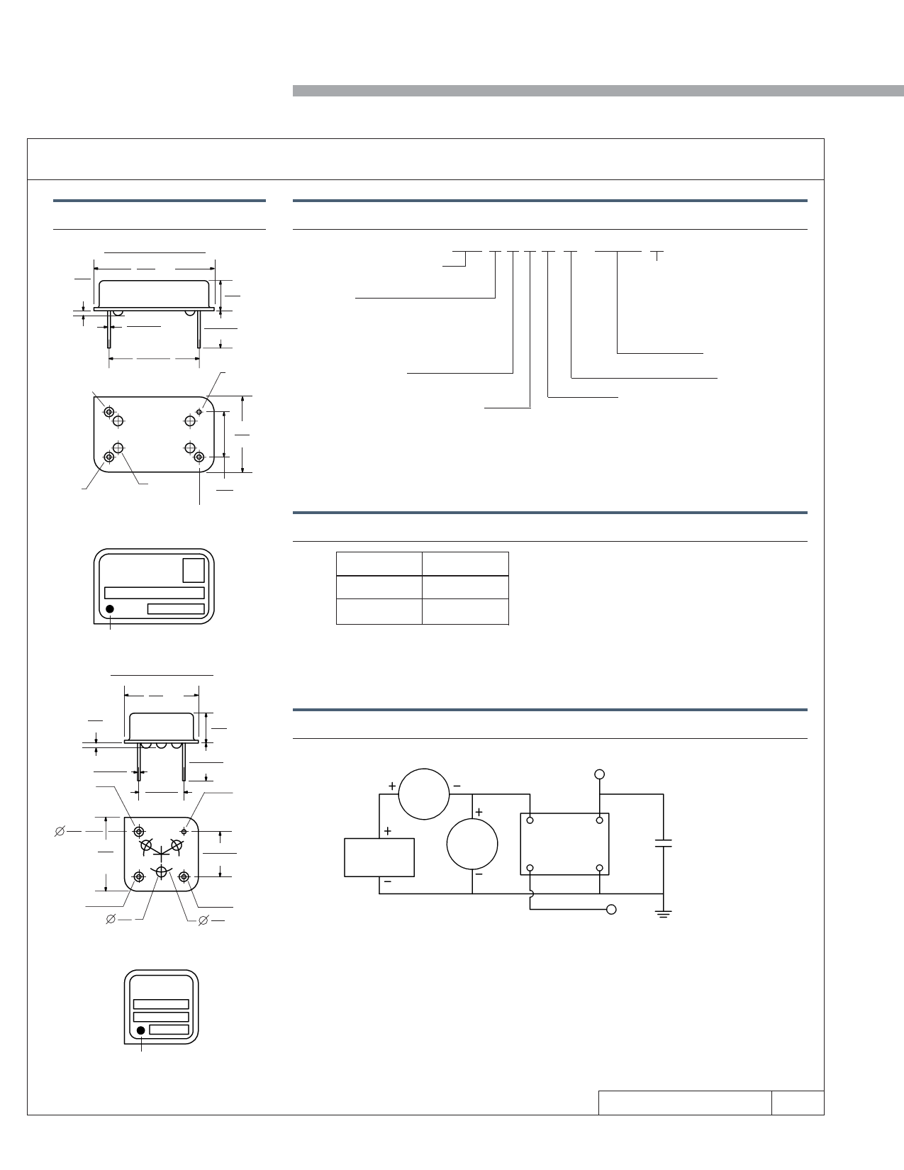
Package Details
FULL SIZE PACKAGE
0.91
21.0
.825
max
.036
max
5.08
.200
max
.46±.08
.018±.003
6.35±0.51
0.25±0.02
Pin 1
Tri-State - NTH
N/C - NCH
15.24±.13
.600±.005
Pin 7
GND
13.0
.510
max
Pin 14
+3.3 VDC
(4) Glass
Insulators
7.75
.305
max
Pin 8 Output
Standard Marking Format**
Includes Date Code, Frequency & Part Number
SARONIX
XTAL OSC
Denotes Pin 1
HALF SIZE PACKAGE
0.91
.036
max
13.0
.510
max
5.08 max
.200
.46±.08
.018±.003
Pin 1
Tri-State - NTH
N/C - NCH
6.35±0.51
0.25±0.02
7.62±.20
.300±.008
Pin 4
GND
1.5
.059
13.0
.510
max
120°
120° 120°
7.62±.20
.300±.008
Pin 8
+3.3 VDC
1.7
.067
Pin 5
6.0 Output
.236
Standard Marking Format**
Includes Date Code, Frequency & Part Number
SARONIX
Part Numbering Guide
NTH 0 8 0 C 3 - 40.0000 (T)
NTH = Pin 1: Tri state, LVCMOS
NCH = Pin 1: N/C, LVCMOS
Symmetry
0 = 40/60% max, 0 to 70°C
2 = 40/60% max, -40 to 85°C
A = 45/55% max, 0 to 70°C, 70 MHz max
C = 45/55% max, -40 to 85°C, 70 MHz max
Packing Method
(T) = Tape & Reel for SMD versions,
full reel increments only, 200pcs (full
size) or 250pcs (half size)
Blank = Bulk
Frequency (MHz)
Frequency Range
3 = 0.5 to 6 MHz
6 = 6+ to 24 MHz
8 = 24+ to 106.25 MHz
3.3V Supply
Package
0 = Full Size, Thru-Hole
9 = Half Size, Thru-Hole
K = Full Size, Gull Wing
J = Half Size, Gull Wing
Stability Tolerance
C = ±100ppm
B = ±50ppm
A = ±25ppm, 0 to +70°C only
AA = ±20ppm, 0 to +70°C only
N = Half Size, Gull Wing, Spanked Leads
S = Full Size, True SMD Adaptor (see separate data sheet for dimensions)
Tri-State Logic Table (NTH only)
Pin 1 Input
Logic 1 or NC
Logic 0 or GND
Pin 8 (5) Output
Oscillation
High Impedance
Required Input Levels on Pin 1:
Logic 1 = 2.2V min
Logic 0 = 0.8V max
Output:
Output:
Internal Pullup Resistance
Control Input:
Oscillation @ VIN, 2.2V min
High Impedance @ VIN, 0.8V max
50KΩ min
Disable Output Delay: 100ns max
Test Circuit
mA
M
POWER
SUPPLY
TEST
POINT
Pin 14 (8)
VDD
Pin 8 (5)
OUT
VM
OSCILLATOR
Pin 1 (1)*
GND
Pin 7 (4)
CL = 50pF, 0.5 to 50 MHz
CL = 30pF, 50+ to 70 MHz
CL = 15pF, 70+ to 106.25 MHz
(Note A)
TRI-STATE INPUT (NTH only)
NOTE A: CL includes probe and fixture capacitance
*( ) Indicates pin numbers for half-size package
Denotes Pin 1
**Exact location of items may vary
All specifications are subject to change without notice.
DS-159 REV D
SaRonix 141 Jefferson Drive • Menlo Park, CA 94025 • USA • 650-470-7700 • 800-227-8974 • Fax 650-462-9894
Share Link: 