MW7IC2750NBR1 Просмотр технического описания (PDF) - Freescale Semiconductor
Номер в каталоге
Компоненты Описание
производитель
MW7IC2750NBR1 Datasheet PDF : 25 Pages
| |||
Freescale Semiconductor
Technical Data
Document Number: MW7IC2750N
Rev. 0, 5/2008
RF Power Field Effect Transistors
N - Channel Enhancement - Mode Lateral MOSFETs
Designed for WiMAX base station applications with frequencies up to
2700 MHz. Suitable for WiMAX, WiBro, BWA, and OFDM multicarrier Class
AB and Class C amplifier applications.
• Typical WiMAX Performance: VDD = 28 Volts, IDQ1 = 160 mA, IDQ2 = 550 mA,
Pout = 8 Watts Avg., f = 2700 MHz, 802.16d, 64 QAM 3/4, 4 bursts,
10 MHz Channel Bandwidth, Input Signal PAR = 9.5 dB @ 0.01% Probability
on CCDF.
Power Gain — 26 dB
Power Added Efficiency — 17%
Device Output Signal PAR — 8.6 dB @ 0.01% Probability on CCDF
ACPR @ 8.5 MHz Offset — - 49 dBc in 1 MHz Channel Bandwidth
Driver Applications
•
TPyoputic=al4WWiMatAtsXAPvegr.,fofr=m2a7n0ce0:MVHDDz,=80228.1V6odlt,s,64IDQQ1A=M136/40,
mA, IDQ2
4 bursts,
= 550 mA,
10 MHz
Channel Bandwidth, Input Signal PAR = 9.5 dB @ 0.01% Probability on
CCDF.
Power Gain — 26 dB
Power Added Efficiency — 11%
Device Output Signal PAR — 9.2 dB @ 0.01% Probability on CCDF
ACPR @ 8.5 MHz Offset — - 57 dBc in 1 MHz Channel Bandwidth
• Capable of Handling 10:1 VSWR, @ 32 Vdc, 2600 MHz, 50 Watts CW
Output Power
• Stable into a 3:1 VSWR. All Spurs Below - 60 dBc @ 1 mW to 80 W CW
Pout
• Pout @ 1 dB Compression Point w 50 Watts CW
Features
• Characterized with Series Equivalent Large - Signal Impedance Parameters
and Common Source Parameters
• On - Chip Matching (50 Ohm Input, DC Blocked)
• Integrated Quiescent Current Temperature Compensation with
Enable/Disable Function (1)
• Integrated ESD Protection
• Greater Negative Gate - Source Voltage Range for Improved Class C Operation
• 225°C Capable Plastic Package
• RoHS Compliant
• In Tape and Reel. R1 Suffix = 500 Units per 44 mm, 13 inch Reel.
VDS1
RFin
VGS1
VGS2
Quiescent Current
Temperature Compensation (1)
RFout/VDS2
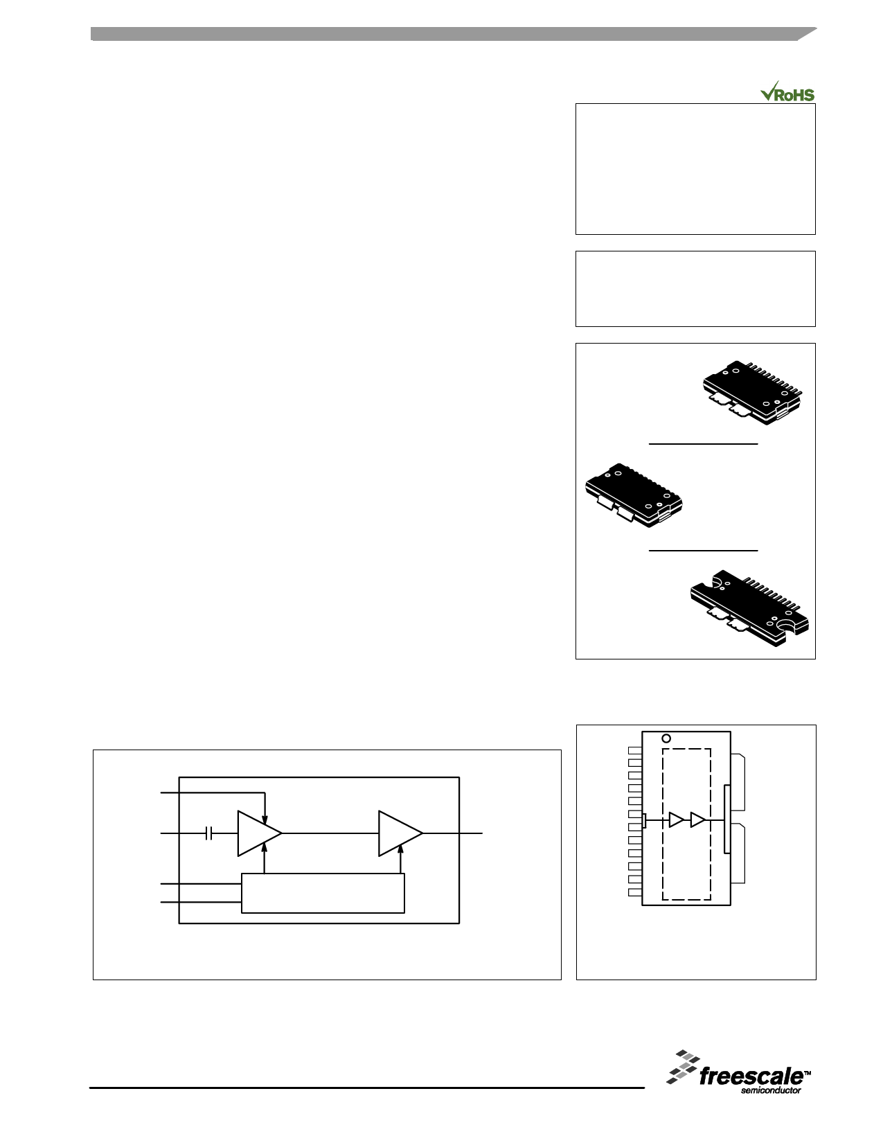
Figure 1. Functional Block Diagram
MW7IC2750NR1
MW7IC2750GNR1
MW7IC2750NBR1
2700 MHz, 8 W AVG., 28 V
WiMAX
LATERAL N - CHANNEL
RF POWER MOSFETs
CASE 1618 - 02
TO - 270 WB - 14
PLASTIC
MW7IC2750NR1
CASE 1621 - 02
TO - 270 WB - 14 GULL
PLASTIC
MW7IC2750GNR1
CASE 1617 - 02
TO - 272 WB - 14
PLASTIC
MW7IC2750NBR1
VDS1 1
VGS2 2
VGS1 3
NC 4
NC 5
RFin 6
RFin 7
NC 8
NC 9
VGS1 10
VGS2 11
VDS1 12
14
RFout /VDS2
13
RFout /VDS2
(Top View)
Note: Exposed backside of the package is
the source terminal for the transistors.
Figure 2. Pin Connections
1. Refer to AN1977, Quiescent Current Thermal Tracking Circuit in the RF Integrated Circuit Family and to AN1987, Quiescent Current
Control for the RF Integrated Circuit Device Family. Go to http://www.freescale.com/rf.
Select Documentation/Application Notes - AN1977 or AN1987.
© Freescale Semiconductor, Inc., 2008. All rights reserved.
RF Device Data
Freescale Semiconductor
MW7IC2750NR1 MW7IC2750GNR1 MW7IC2750NBR1
1
Share Link: 