MV8870 Просмотр технического описания (PDF) - Zarlink Semiconductor Inc
Номер в каталоге
Компоненты Описание
производитель
MV8870 Datasheet PDF : 12 Pages
| |||
MV8870/MV8870-1
APPLICATIONS
A simple application circuit is shown in Fig.7. This has a
symmetric guard time circuit, a single-ended analog input and
a dedicated crystal oscillator.
GUARD TIME ADJUSTMENT
In many situations not requiring seperate selection of tone
duration and interdigit pause, the simple steering circuit shown
in Fig.7 is applicable. Component values are chosen according
to the formulae (see Figs. 4, 8a and 8b):-
tREC = tDP + tGTP
tlD = tDA + tGTA
The value of tDP is a device parameter (see Dynamic
Characteristics and Fig.5) and tREC is the minimum signal
duration to be recognised by the receiver. Likewise tDA is a
device parameter (Fig.5) and tlD is the minimum time taken to
recognise an interdigit pause. A value for C2 of 0.1µ-F is
recommended for most applications, leaving R3 to be selected
by the designer.
Different steering arrangements may be used to select
independantly the guard times for tone present (tGTP) and tone
absent (tGTA). This may be necessary to meet system
specifications which place both accept and reject limits on both
tone duration and interdigit pause. Guard Time adjustment
also allows the designer to tailor system parameters such as
talk-off and noise immunity. Increasing tREC improves talk-off
performance since it reduces the probability that tones
simulated by speech will maintain signal conditions long
enough to be registered. Alternatively a relatively short tREC
wim a long tlD would be appropriate for extremely noisy
environments where fast acquisition time and immunity to tone
drop-outs are required. Design information for guard time
adjustment is shown in Figs. 8a and 8b.
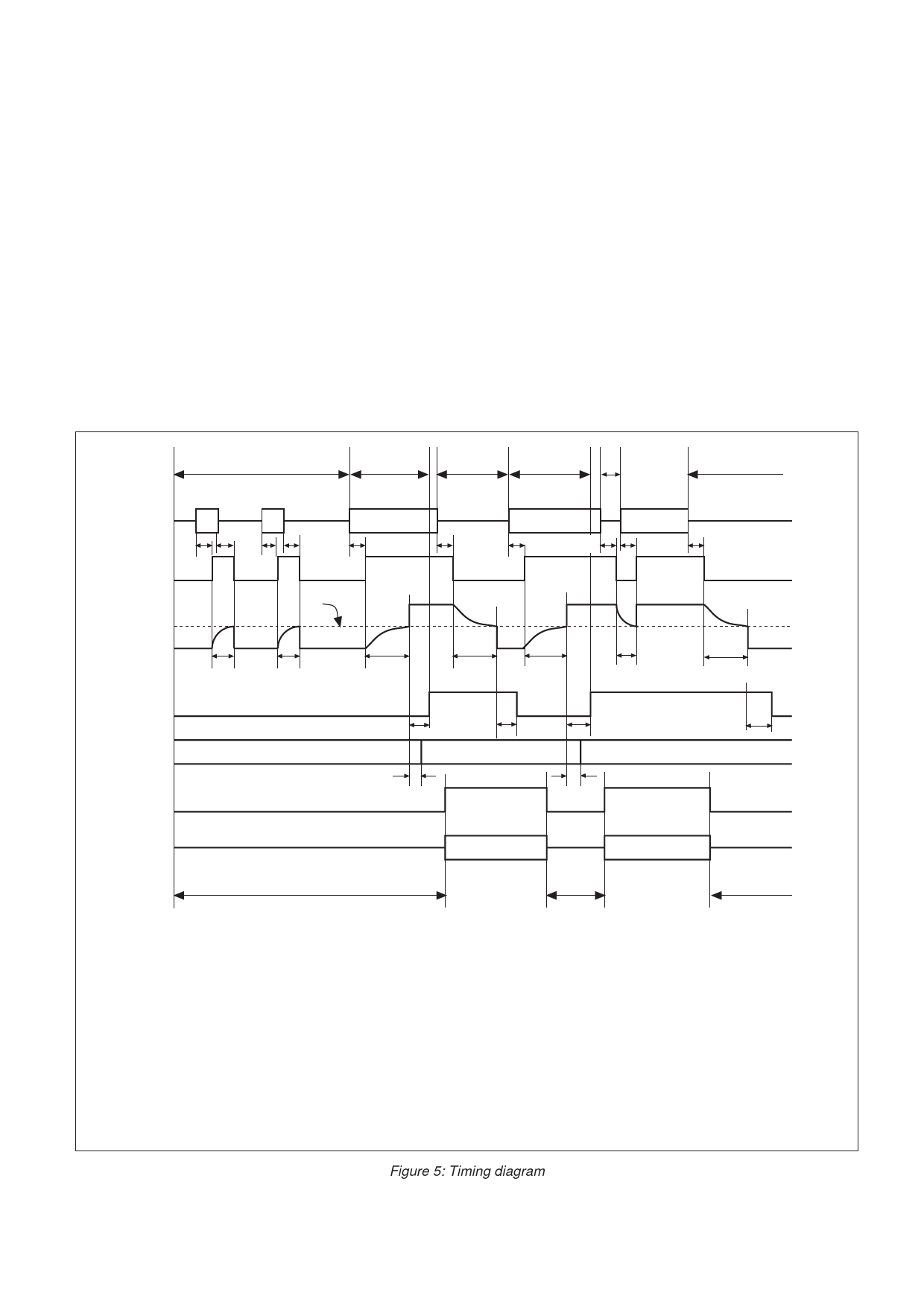
A
B
C
E
F
G
VIN
tDA
tDP
tDP
ESt
St/GT
TONE N
tDA
tDP
VTSt
TONE N + 1
TONE N + 1
tDA
tDA
tDP
tDA
tDP
StD
CODE
CONVERTER
LATCH
OUTPUTS
TOE
t < tGTP t < tGTP
t = tGTP
t = tGTA
t = tGTP
t < tGTA
t = tGTA
tPStD
DECODED TONE N-1
tPQ
tPStD
TONE N
tPStD
tPQ
TONE N + 1
tPStD
Q1 - Q4
D
TONE N
TONE N + 1
D
D
EXPLANATION OF EVENTS
A, Tone bursts detected, but tone duration invalid and output latch unchanged.
B. Tone N detected, tone duration valid, output latch updated and new data signalled by
StD.
C. End of tone N detected, tone absent duration valid, but output latch updated until next
valid tone.
D. Outputs switched to high impedance.
E. Tone N + 1 detected, tone duration valid, tone decoded, output latch updated
(although outputs are currently high impedance) and new data signalled by StD.
F. Acceptable dropout of tone N + 1, tone absent duration invalid, StD and output latch
unchanged.
G. End of tone N + 1 detected, tone absent duration valid, StD goes low but output latch
not updated until next valid tone.
NOTES
1. tDP time for valid tone present is
a device parameter (see Electrical
Characteristics).
2. tDA time for valid tone absent is
a device parameter (see Electrical
Characteristics).
3. tGTP and tGTA are adjustable via
external RC network at pins 16
and 17 (see Fig. 4).
4. tPSID and tPQ are propogation
delays given in Electrical
Characteristics.
Figure 5: Timing diagram
3
Share Link: 