MN12511 Просмотр технического описания (PDF) - Panasonic Corporation
Номер в каталоге
Компоненты Описание
производитель
MN12511 Datasheet PDF : 9 Pages
| |||
MN12511
s Operational Description (continued)
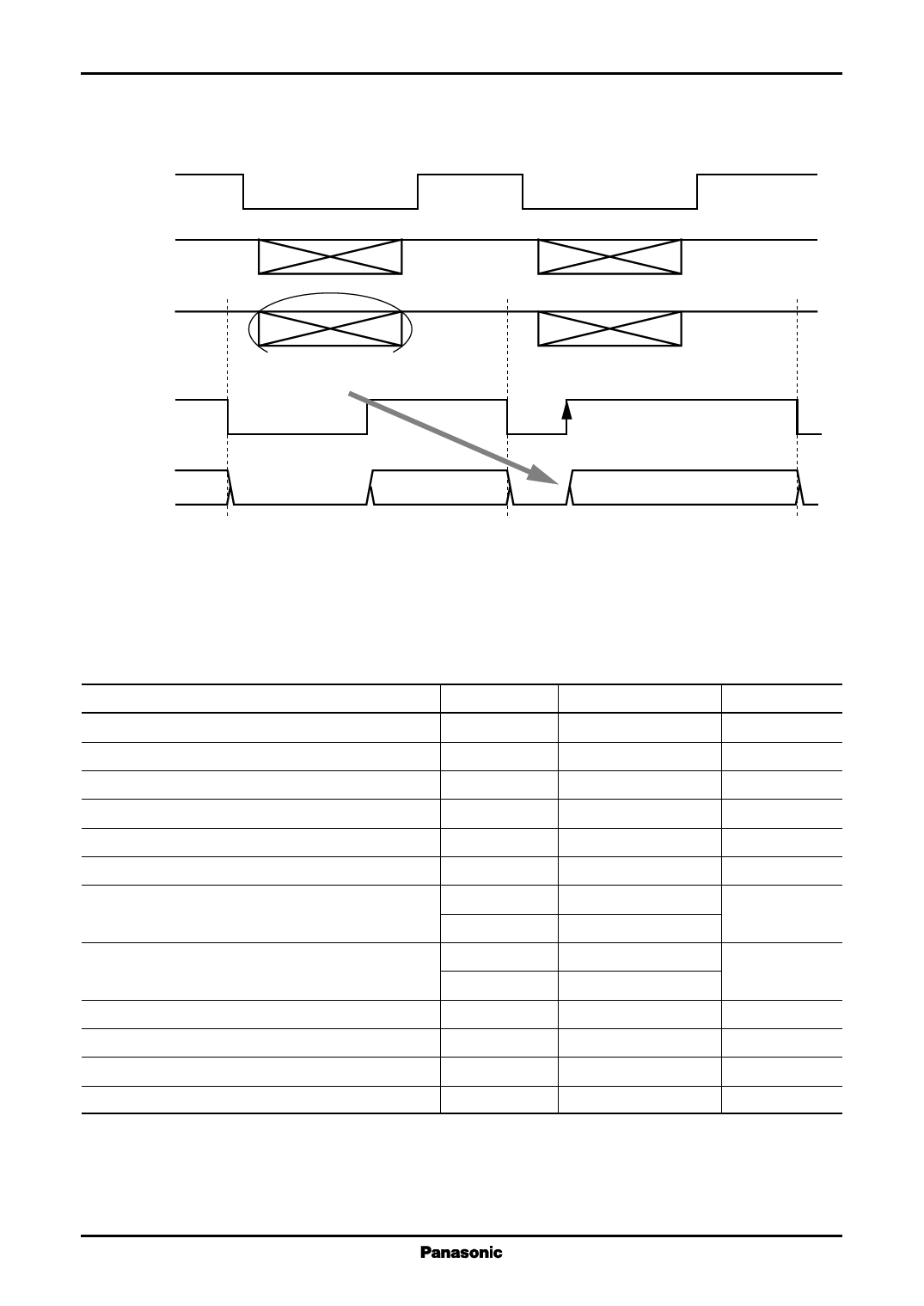
• Display Timing
NCE
NSCK
NSDI
OE
Serial data transferred to
the 16-bit shift register
D0 to Dn
Microcontroller Peripheral LSIs
Display start
Note) 1. The OE pin should be set low each time the display is changed.
2. If the fluorescent display control input (OE) is set low during a serial data transfer, the MN12511 will detect an
incorrect transfer and output the VPP level from all the high-voltage output ports.
s Electrical Characteristics
1. Absolute Maximum Ratings at VSS = 0 V, Ta = 25 °C±2 °C
Parameter
Symbol
Rating
Unit
Supply voltage (digital power supply)
VDD
− 0.3 to +7.0
V
Supply voltage (High-voltage output power supply)
VPP
VDD− 45 to VDD+0.3
V
Input voltage
VI1
VSS− 0.3 to VDD+0.3
V
Output voltage
VO1
VSS− 0.3 to VDD+0.3
V
I/O voltage
VIO1
VSS− 0.3 to VDD+0.3
V
High-voltage output pin voltage
VIO2
− 40 to VDD+0.3
V
Normal pin peak output current
IOH(peak)
−10
mA
IOL(peak)
30
Normal pin average output current
IOH(ave)
−5
mA
IOL(ave)
15
High-voltage output pin output current
IOH
−30
mA
Allowable power dissipation
PT
300
mW
Operating temperature
Topr
−10 to +70
°C
Storage temperature
Tstg
−55 to +125
°C
Note) 1. These values are limiting values under which the device will not be destroyed. Operation is not guaranteed within these
ranges.
2. These values are limiting values such that the device will not be destroyed if voltages within these ranges are applied to the
pins. Operation is not guaranteed within these ranges.
3. Applies to any 100 ms period.
4
Share Link: 