MK2058-01 Просмотр технического описания (PDF) - Integrated Circuit Systems
Номер в каталоге
Компоненты Описание
производитель
MK2058-01 Datasheet PDF : 10 Pages
| |||
MK2058-01
Communications Clock Jitter Attenuator
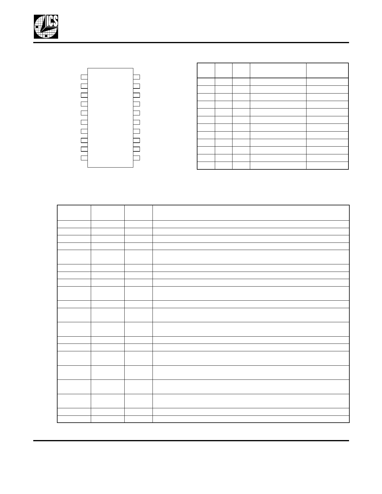
Pin Assignment
X1 1
VDD 2
VDD 3
VDD 4
VIN 5
GND 6
GND 7
GND 8
CHGP 9
ISET 10
20 X2
19 GND
18 ISEL
17 ICLK1
16 ICLK2
15 SEL0
14 CLK
13 NC
12 SEL1
11 SEL2
20 pin 300 mil SOIC
Pin Descriptions
Output Clock Selection Table
SEL2 SEL1 SEL0
000
001
010
011
M0 0
M0 1
M1 0
M1 1
100
101
110
111
Input / Output
Range
4.4 to 8.79 kHz
1 to 1.6 MHz
1.6 to 2.7 MHz
2.7 to 4.5 MHz
6.6 to 13.2 kHz
7.8 to 15.734kHz
64 to 70 kHz
105 to 210 kHz
4.0 to 6.8 MHz
5.5 to 9 MHz
8.5 to 13.5 MHz
13.5 to 27 MHz
Crystal
Frequency
3072 x ICLK
16 x ICLK
10 x ICLK
6 x ICLK
2048 x ICLK
1716 x ICLK
384 x ICLK
128 x ICLK
4 x ICLK
3 x ICLK
2 x ICLK
1 x ICLK
Note: For SEL input pin programming:
0 = GND, 1 = VDD, M = Floating
Pin
Number
1
2
3
4
5
6
7
8
9
10
11
12
13
14
15
16
17
18
19
20
Pin
Name
X1
VDD
VDD
VDD
VIN
GND
GND
GND
CHGP
ISET
SEL2
SEL1
NC
CLK
SEL0
ICLK2
ICLK1
ISEL
GND
X2
Pin
Type
-
Power
Power
Power
Input
Power
Power
Power
Output
-
Input
Input
Input
Output
Input
Input
Input
Input
Power
-
Pin Description
Crystal Input. Connect this pin to the specified crystal.
Power Supply. Connect to +3.3V.
Power Supply. Connect to +3.3V.
Power Supply. Connect to +3.3V.
VCXO Control Voltage Input. Connect this pin to CHGP pin and the external
loop filter as shown in this data sheet.
Connect to ground
Connect to ground
Connect to ground
Charge Pump Output. Connect this pin to the external loop filter and to pin
VIN.
Charge pump current setting node, connection for setting resistor.
Output Frequency Selection Pin 2. Determines output frequency as per table
above. Internally biased to VDD/2.
Output Frequency Selection Pin 1. Determines output frequency as per table
above. Internal pull-up.
No Internal Connection.
Clock Output
Output Frequency Selection Pin 0. Determines output frequency as per table
above. Internal pull-up.
Input Clock Connection 2. Connect an input reference clock to this pin. If
unused, connect to ground.
Input Clock Connection 1. Connect an input reference clock to this pin. If
unused, connect to ground.
Input Selection. Used to select which reference input clock is active. Low input
level selects ICLK1, high input level selects ICLK2. Internal pull-up.
Connect to ground.
Crystal Output. Connect this pin to the specified crystal.
MDS 2058-01 B
2
Revision 071001
Integrated Circuit Systems, Inc. q 525 Race Street, San Jose, CA 95126 q tel (408) 295-9800 q www.icst.com
Share Link: 