MCRF450 Просмотр технического описания (PDF) - Microchip Technology
Номер в каталоге
Компоненты Описание
производитель
MCRF450 Datasheet PDF : 50 Pages
| |||
MCRF450/451/452/455
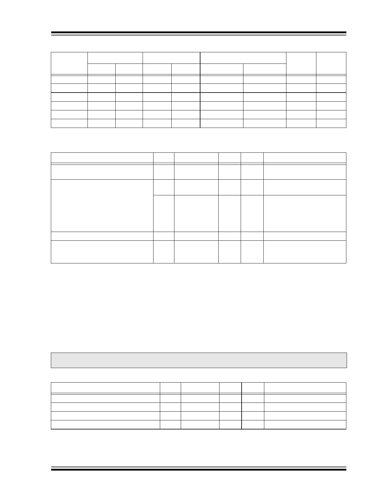
TABLE 2-4: PAD COORDINATES (MICRONS)
Pad Name
Lower
Left X Left Y
Upper
Right X Right Y
Passivation Openings
Pad Width
Pad Height
Ant. Pad A -853.50 -992.10 -764.50 -903.10
89.00
89.00
Ant. Pad B 759.50 -993.70 848.50 -904.70
89.00
VSS
769.10 977.90 858.10 1066.90
89.00
VDD
-839.50 45.50 -750.50 134.50
89.00
CLK
721.10 77.80 810.10 166.80
89.00
FCLK
-821.50 910.70 -732.50 999.70
89.00
Note 1: All coordinates are referenced from the center of the die.
89.00
89.00
89.00
89.00
89.00
Pad
Pad
Center X Center Y
-809.00
804.00
813.60
-795.00
765.60
-777.00
-947.60
-949.20
1022.40
90.00
122.30
955.20
TABLE 2-5: DIE MECHANICAL DIMENSIONS
Specifications
Min
Typ
Max Unit
Comments
Bond pad opening
—
3.5 x 3.5
—
mil Note 1, Note 2
—
89 x 89
—
µm
Die backgrind thickness
7.5
190.5
8
203.2
8.5
215.9
mil Sawed 8” wafer on frame
µm (option = WF) (Note 3)
10
11
12
mil • Bumped, sawed 8” wafer
on frame (option = WFB)
254
279.4
304.8 µm • Unsawed wafer (option = W)
• Unsawed 8” bumped
wafer (option = WB), (Note 3)
Die passivation thickness (multilayer)
—
1.3
—
µm Note 4
Die Size:
Die size X*Y before saw (step size)
Die size X*Y after saw
— 1904 x 2340.8 —
— 1840.5 x 2277.3 —
µm —
µm —
Note 1: The bond pad size is that of the passivation opening. The metal overlaps the bond pad passivation by at
least 0.1 mil.
2: Metal Pad Composition is 98.5% Aluminum with 1% Si and 0.5% Cu.
3: As the die thickness decreases, susceptibility to cracking increases. It is recommended that the die be as
thick as the application will allow.
4: The Die Passivation Thickness (1.3 µm) can vary by device depending on the mask set used. The
passivation is formed by:
- Layer 1: Oxide (undoped oxide)
- Layer 2: PSG (doped oxide)
- Layer 3: Oxynitride (top layer)
5: The conversion rate is 25.4 µm/mil.
Notice: Extreme care is urged in the handling and assembly of die products since they are susceptible to
mechanical and electrostatic damage.
TABLE 2-6: WAFER MECHANICAL SPECIFICATIONS
Specifications
Min
Typ
Max
Wafer Diameter
Die separation line width
Dice per wafer
Batch size
—
8
—
—
80
—
—
6,600
—
—
24
—
Unit
inch
µm
die
wafer
Comments
2003 Microchip Technology Inc.
DS40232H-page 7
Share Link: 