MBF9041BB(2000) Просмотр технического описания (PDF) - Oki Electric Industry
Номер в каталоге
Компоненты Описание
производитель
MBF9041BB Datasheet PDF : 10 Pages
| |||
1Semiconductor
FEDL9041BB-01
MBF9041BB
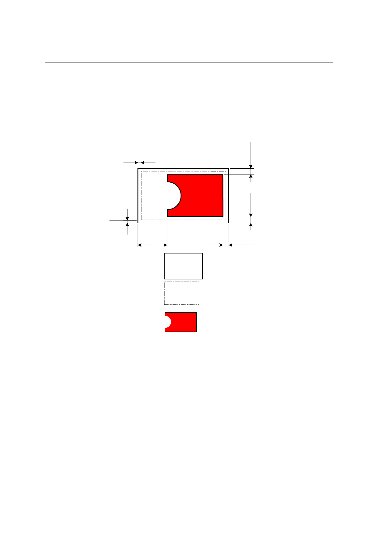
RECOMMENDATION FOR SOLDER PAD PATTERN
The solder pad pattern should be designed by customers because it depends on the electrical
performance of the customers’ system. Following is an example of solder pad pattern which is used in
OKI’s package evaluation board. Please be noted that this is for reference purpose only.
25 µm
0.1 mm
25 µm
0.5 mm
0.1 mm
0.1 mm
PCB pad pattern
Metal mask pattern
Pad of Device
Please pay attention to the following items to maintain electrical performance.
(1) Metal mask pattern for cream solder should be 25 µm smaller on each side. Metal mask is 0.15 mm in
thickness.
(2) As the impedance of Tx, Rx, ANT is designed for 50 Ω, please consider this for the design of mother board.
(3) The performance of these devices is assured when GND pad (Pin 17) is connected. GND pad (Pin 17) should
be soldered in the same way as above.
9/10
Share Link: 