MAX9711ETC(2008) Просмотр технического описания (PDF) - Maxim Integrated
Номер в каталоге
Компоненты Описание
производитель
MAX9711ETC Datasheet PDF : 13 Pages
| |||
3W Mono/Stereo BTL Audio Power Amplifiers
with Shutdown
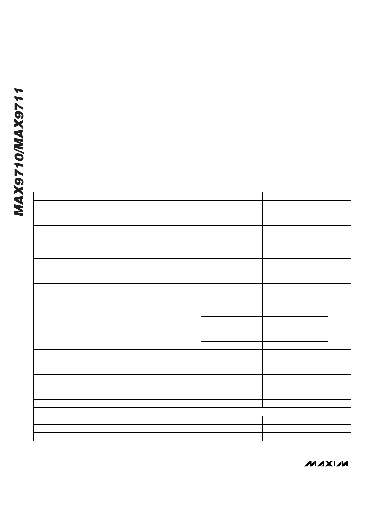
ABSOLUTE MAXIMUM RATINGS
VDD to GND, PGND ...............................................................+6V
PVDD to VDD .......................................................................±0.3V
PGND to GND.....................................................................±0.3V
All Other Pins to GND.................................-0.3V to (VDD + 0.3V)
Continuous Input Current (into any pin
except power supply and output pins).........................±20mA
Continuous Power Dissipation (TA = +70°C)
12-Pin Thin QFN (derate 16.9mW/°C above +70°C) ....1349mW
20-Pin Thin QFN (derate 20.8mW/°C above +70°C) ....1667mW
Operating Temperature Range............................-40°C to +85°C
Storage Temperature Range .............................-65°C to +150°C
Junction Temperature ......................................................+150°C
Lead Temperature (soldering, 10s) .................................+300°C
Stresses beyond those listed under “Absolute Maximum Ratings” may cause permanent damage to the device. These are stress ratings only, and functional
operation of the device at these or any other conditions beyond those indicated in the operational sections of the specifications is not implied. Exposure to
absolute maximum rating conditions for extended periods may affect device reliability.
ELECTRICAL CHARACTERISTICS
(VDD = PVDD = 5.0V, VGND = VPGND = VMUTE = 0V, V SHDN = 5V, RIN = RF = 15kΩ, RL = ∞. TA = TMIN to TMAX, unless otherwise
noted. Typical values are at TA = +25°C.) (Note 1)
PARAMETER
SYMBOL
CONDITIONS
MIN TYP
Supply Voltage Range
Quiescent Supply Current
(IVDD + IPVDD)
Shutdown Supply Current
VDD/PVDD
IDD
I SHDN
Inferred from PSRR test
MAX9710
MAX9711
SHDN = GND
4.5
12
7
0.5
Turn-On Time
tON
CBIAS = 1µF (10% of final value)
CBIAS = 0.1µF (10% of final value)
300
30
Thermal Shutdown Threshold
160
Thermal Shutdown Hysteresis
15
OUTPUT AMPLIFIERS
Output Offset Voltage
Power-Supply Rejection Ratio
VOS
PSRR
VOUT_+ - VOUT_-, AV = 2
VRIPPLE = 200mVP-P
(Note 2)
VDD = 4.5V to 5.5V
f = 1kHz
f = 20kHz
±2
82
100
87
74
Output Power
Total Harmonic Distortion Plus
Noise
Signal-to-Noise Ratio
POUT
THD+N
SNR
fIN = 1kHz,
THD+N < 1%
RL = 8Ω
RL = 4Ω
RL = 3Ω
fIN = 1kHz, BW =
22Hz to 22kHz
POUT = 1.2W, RL = 8Ω
POUT = 2W, 4Ω
RL = 8Ω, VOUT = 2.8VRMS, BW = 22Hz to 22kHz
1.1
1.4
2.6
3
0.005
0.01
95
Slew Rate
SR
1.6
Maximum Capacitive Load Drive
CL
No sustained oscillations
1
Crosstalk
fIN = 10kHz
77
BIAS VOLTAGE (BIAS)
BIAS Voltage
VBIAS
2.35 2.5
Output Resistance
RBIAS
50
DIGITAL INPUTS (MUTE, SHDN)
Input Voltage High
VIH
2
Input Voltage Low
VIL
Input Leakage Current
IIN
Note 1: All devices are 100% production tested at +25°C. All temperature limits are guaranteed by design.
Note 2: PSSR is specified with the amplifier inputs connected to GND through RIN and CIN.
MAX
5.5
30
17
30
±14
2.65
0.8
±1
UNITS
V
mA
µA
ms
°C
°C
mV
dB
W
%
dB
V/µs
nF
dB
V
kΩ
V
V
µA
2 _______________________________________________________________________________________
Share Link: 