SST38VF166-70-4C-EK Просмотр технического описания (PDF) - Silicon Storage Technology
Номер в каталоге
Компоненты Описание
производитель
SST38VF166-70-4C-EK Datasheet PDF : 50 Pages
| |||
16 Megabit FlashBank Memory
SST38VF166
Data Sheet
Common Flash Interface (CFI)
The SST38VF166 also contains the CFI information in
each bank, to describe the characteristics of that bank. See
Tables 8 through 16 for the CFI contents for each bank.
Both flash banks use the same information, as each bank
operates the same. The E2 bank contains the applicable
information for that bank.
In order to obtain the CFI information, the CFI memory
space is accessed by using the CFI entry command. For
details, see Table 6 or 7 for software operation and Figures
33, 34, or 35 for timing waveforms.
CFI Mode Exit
In order to return to the standard Read mode, the CFI
mode must be exited. Exit is accomplished by issuing the
CFI exit command, which returns the device to normal
operation. This command may also be used to reset the
device to the Read mode after any inadvertent transient
condition that apparently causes the device to behave
abnormally, e.g., not read correctly. For details, see Table 6
or 7 for software operation and Figures 36, 37, or 38 for tim-
ing waveforms.
CFI is specified for byte wide information. Since the
SST38VF166 is organized word wide, the first byte (2 nib-
bles) of each CFI word is always 00H.
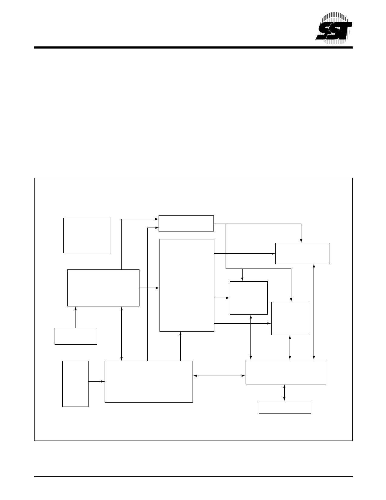
FUNCTIONAL BLOCK DIAGRAM
Charge
Pump &
Vref.
Address Buffer
and Latches
Y - Decoder
X - Decoder
A18 - A0
OE#
BE#1
BE#2
BE#3
WE#
Control Logic
4K x 16
E2 Bank
512K x 16
Flash
Bank 1
512K x 16
Flash
Bank 2
I/O Buffers and
Data Latches
DQ15 - DQ0
327 ILL F02.1
©2001 Silicon Storage Technology, Inc.
7
327-3 2/01
S71065
Share Link: 