M68AR024D Просмотр технического описания (PDF) - STMicroelectronics
Номер в каталоге
Компоненты Описание
производитель
M68AR024D Datasheet PDF : 19 Pages
| |||
M68AR024D
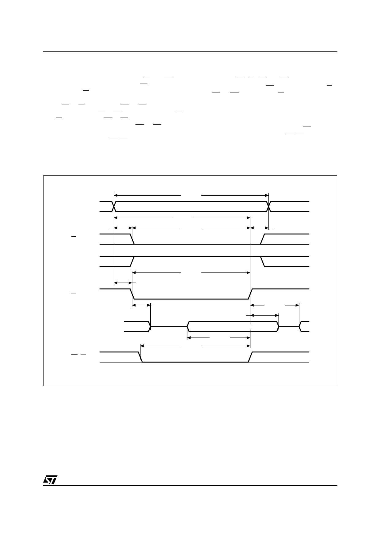
Write Mode
The M68AR024D, when Chip Select (E2) is High,
is in the Write Mode whenever the W and E1 are
Low. Either the Chip Enable Input (E1) or the Write
Enable input (W) must be de-asserted during Ad-
dress transitions for subsequent write cycles.
When E1 or W is Low, and UB or LB is Low, write
cycle begins on the W or E1 falling edge. When E1
and W are Low, and UB = LB = High, write cycle
begins on the first falling edge of UB or LB. There-
fore, address setup time is referenced to Write En-
able, Chip Enables and UB/LB as tAVWL, tAVEL and
tAVBL respectively, and is determined by the latter
occurring falling edge.
The Write cycle can be terminated by the earlier
rising edge of E1, W, UB and LB.
If the Output is enabled (E1 = Low, E2 = High, G =
Low, LB or UB = Low), then W will return the out-
puts to high impedance within tWLQZ of its falling
edge. Care must be taken to avoid bus contention
in this type of operation. Data input must be valid
for tDVWH before the rising edge of Write Enable,
or for tDVEH before the rising edge of E1 or for tD-
VBH before the rising edge of UB/LB, whichever
occurs first, and remain valid for tWHDX, tEHDX and
tBHDX respectively.
Figure 10. Write Enable Controlled, Write AC Waveforms
A0-A19
tAVEL
E1
E2
W
DQ0-DQ15
UB, LB
tAVAV
VALID
tAVWH
tELWH
tWHAX
tAVWL
tWLWH
tWLQZ
tBLBH
tWHDX
DATA INPUT
tDVWH
tWHQX
AI05991
11/19
Share Link: 