MAX682 Просмотр технического описания (PDF) - Maxim Integrated
Номер в каталоге
Компоненты Описание
производитель
MAX682 Datasheet PDF : 12 Pages
| |||
3.3V-Input to Regulated 5V-Output
Charge Pumps
Detailed Description
The MAX682/MAX683/MAX684 charge pumps provide
a regulated 5V output from a 2.7V to 5.5V input. They
deliver a maximum of 250mA, 100mA, or 50mA load
current, respectively. Designed specifically for com-
pact applications, a complete regulator circuit requires
only three small external capacitors and one resistor.
An externally adjustable switching frequency and inno-
vative control scheme allow the circuit to be optimized
for efficiency, size, or output noise. The devices also
contain a shutdown feature.
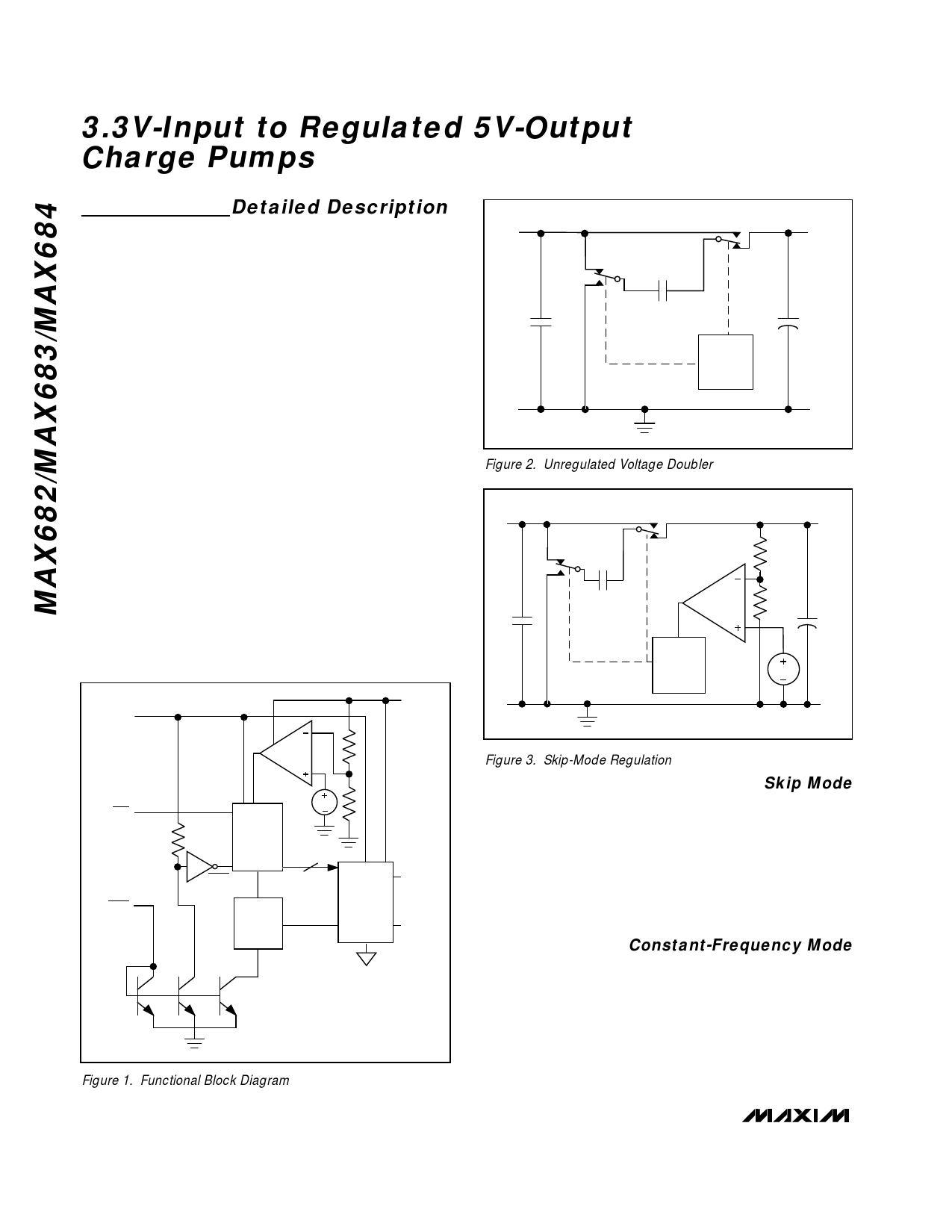
The MAX682/MAX683/MAX684 consist of an error
amplifier, a 1.23V bandgap reference, an internal resis-
tive feedback network, an oscillator, high-current MOS-
FET switches, and shutdown and control logic (Figure
1). Figure 2 shows an idealized unregulated charge-
pump voltage doubler. The oscillator runs at a 50%
duty cycle. During one half of the period, the transfer
capacitor (CX) charges to the input voltage. During the
other half, the doubler stacks the voltage across CX
and the input voltage, and transfers the sum of the two
voltages to the output filter capacitor (COUT). Rather
than simply doubling the input voltage, the
MAX682/MAX683/MAX684 provide a regulated fixed
output voltage (5V) using either skip mode or constant-
frequency mode. Skip mode and constant-frequency
mode are externally selected via the SKIP input pin.
OUT
IN
IN
S1
CIN
S2
CX
OSC
Figure 2. Unregulated Voltage Doubler
IN
S1
S2
CX
CIN
EN
OSCILLATOR
OUT
COUT
OUT
SKIP
SHDN
1.23V
CONTROL
LOGIC
SHDN
EN
OSC
CXP
SWITCHES
CXN
PGND
Figure 1. Functional Block Diagram
Figure 3. Skip-Mode Regulation
Skip Mode
In skip mode (SKIP = low), the error amplifier disables
switching when it detects an output higher than 5V. The
device then skips switching cycles until the output volt-
age drops. Then the error amplifier reactivates the
oscillator. Figure 3 illustrates the regulation scheme.
This regulation method minimizes operating current
because the device does not switch continuously. SKIP
is a logic input and should not remain floating.
Constant-Frequency Mode
When SKIP is high, the charge pump runs continuously
at the selected frequency. Figure 4 shows a block dia-
gram of the device in constant-frequency mode. The
error amplifier controls the charge on CX by driving the
gate of the N-channel FET. When the output voltage
falls, the gate drive increases, resulting in a larger volt-
age across CX. This regulation scheme minimizes out-
put ripple. Since the device switches continuously, the
6 _______________________________________________________________________________________
Share Link: 