MAX44269 Просмотр технического описания (PDF) - Maxim Integrated
Номер в каталоге
Компоненты Описание
производитель
MAX44269 Datasheet PDF : 14 Pages
| |||
MAX44269
1.3mm x 1.3mm, Low-Power
Dual Comparator
Logic-Level Translator
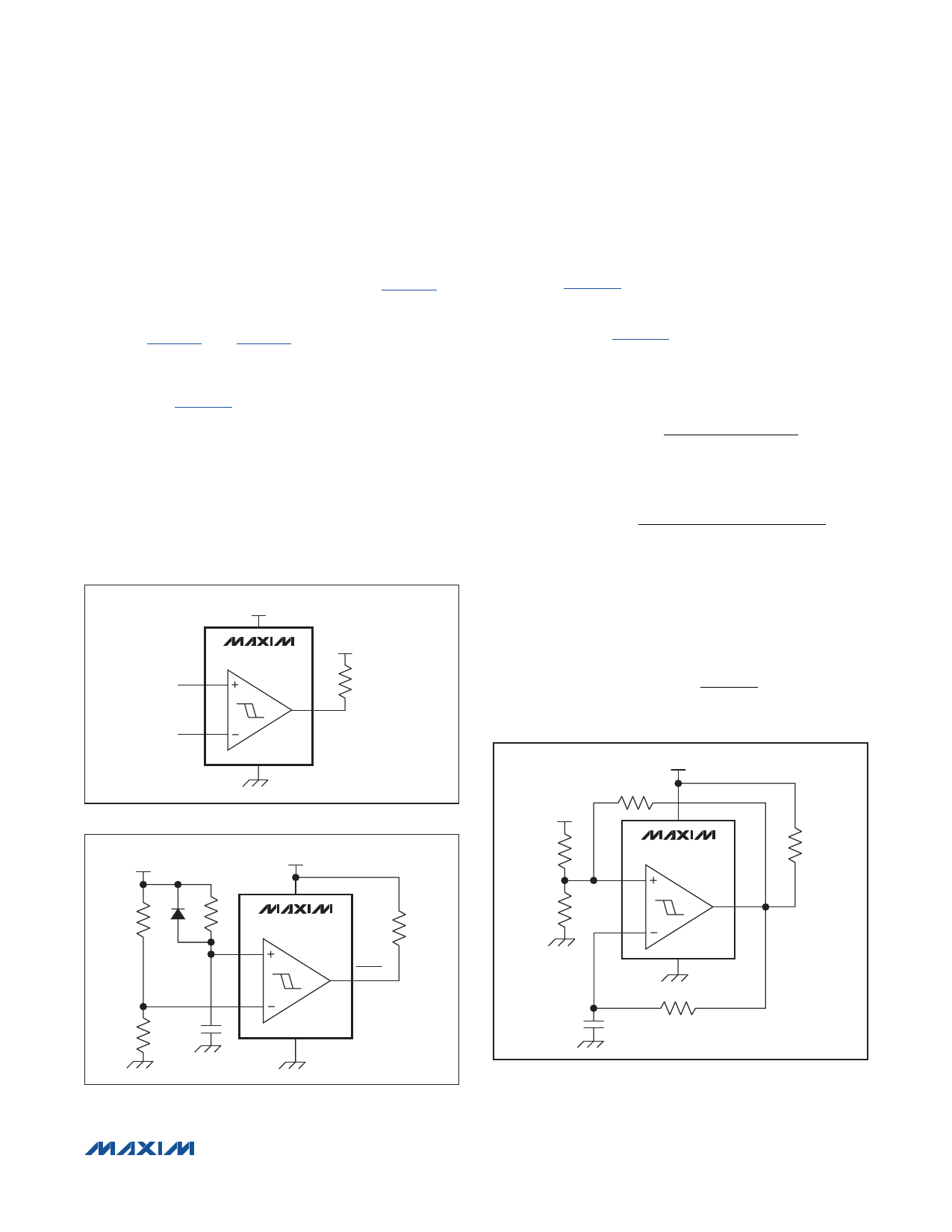
Due to the open-drain output of the IC, the device can
translate between two different logic levels (Figure 4). If
the internal 4 mV hysteresis is not sufficient, then exter-
nal resistors can be added to increase the hysteresis as
shown in Figure 2 and Figure 3.
Power-On Reset Circuit
The IC can be used to make a power-on reset circuit as
displayed in Figure 5. The positive input provides the
ratiometric reference with respect to the power supply
and is created by a simple resistive divider. Choose
reasonably large values to minimize the power consump-
tion in the resistive divider. The negative input provides
the power-on delay time set by the time constant of the
RC circuit formed by R2 and C1. This simple circuit can
be used to power up the system in a known state after
ensuring that the power supply is stable. Diode D1 pro-
vides a rapid reset in the event of unexpected power loss.
Relaxation Oscillator
The IC can also be used to make a simple relaxation
oscillator (Figure 6). By adding the RC circuit R5 and
C1, a standard Schmidt Trigger circuit referenced to
a set voltage is converted into an astable multivibra-
tor. As shown in Figure 7, IN- is a sawtooth waveform
with capacitor C1 alternately charging and discharging
through resistor R5. The external hysteresis network
formed by R1 to R4 defines the trip voltages as:
VT
_RISE
=
VCC
R2R3
R3 x R4
+ R2R4 +
R3R4
R4R5(R1+ R2 + R3)
V T _FALL
=
VCC
R4R5
(R1
+ R1R3R4
+ R2 + R3)
+
R1R3R4
+ R2(R1R3 + R3R5 + R1R5)
VCC
MAX44269
VIN
VPULL
R1
OUT
VREF
GND
Figure 4. Logic-Level Translator
VCC
VCC
R3 D1 R2
MAX44269
R1
RESET
R4
C1
GND
Figure 5. Power-On Reset Circuit
Using the basic time domain equations for the charging
and discharging of an RC circuit, the logic-high time,
logic-low time, and frequency can be calculated as:
tLOW
=
R5C1
ln
V T _FALL
V T _RISE
VCC
R2
R4
VCC
R3
MAX44269
R1
OUT
GND
R5
C1
Figure 6. Relaxation Oscillator
���������������������������������������������������������������� Maxim Integrated Products 10
Share Link: 