MAX3866 Просмотр технического описания (PDF) - Maxim Integrated
Номер в каталоге
Компоненты Описание
производитель
MAX3866 Datasheet PDF : 12 Pages
| |||
2.5Gbps, +3.3V Combined
Transimpedance/Limiting Amplifier
Applications Information
Converting Average Optical Power
to Signal Amplitude
Many of the MAX3866’s specifications relate to input
signal amplitude. When working with fiber optic
receivers, the input is usually expressed in terms of
average optical power and extinction ratio. The rela-
tions given in Table 1 are helpful for converting optical
power to input signal when designing with the
MAX3866.
In an optical receiver, the input current to the transim-
pedance amplifier can be found by multiplying the
power relationships in Table 1 with the photodiode
responsivity.
Wire Bonding
Make corrections to the die with gold wire only, using
ball bonding techniques. Die pad size is 4mils (100µm)
square and die thickness is 12mils (~300µm).
Layout Techniques
The MAX3866’s performance can be greatly affected
by circuit board layout and design. Use good high-fre-
quency design techniques, including minimizing
ground inductances and using fixed-impedance trans-
mission lines on all data signals.
Table 1. Optical-Power Relations*
PARAMETER SYMBOL
RELATION
Average
Power
PAVE PAVE = (P0 + P1) / 2
Extinction
Ratio
re
re = P1 / P0
Optical Power
of a “1”
Optical Power
of a “0”
P1
P1 = 2PAVE re
re + 1
P0
P0 = 2PAVE / (re +1)
Signal
Amplitude
PIN
PIN = P1 - P0 = 2PAVE (re - 1)
(re + 1)
*Assuming a 50% average input mark density.
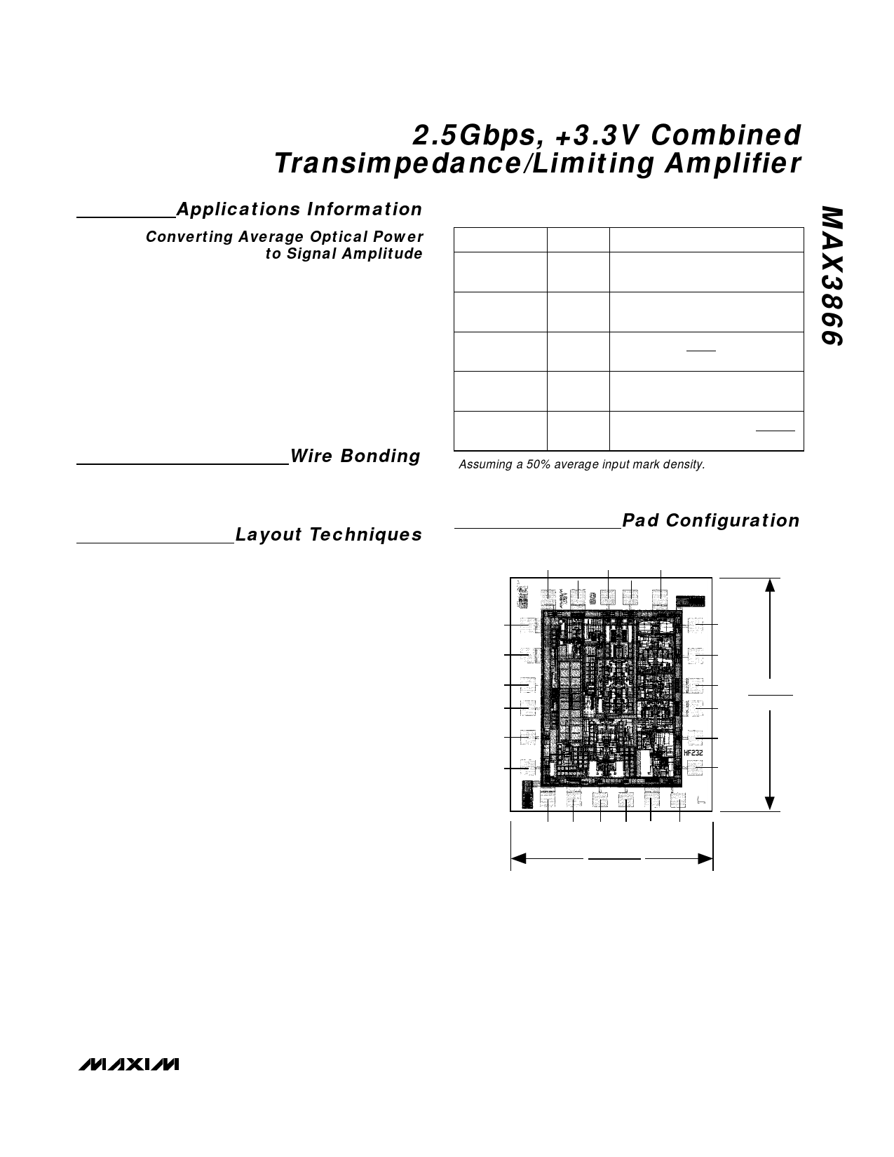
Pad Configuration
LOP
OUT+
GND
GND
OUT-
VCCD
VCCD
VCCS
VCCS
CHF+
CHF-
CPD+
CPD-
GND 0.066"
GND (1.68mm)
INV
PDC
FIL GND IN+ IN- GND N.C.
0.057"
(1.45mm)
TRANSISTOR COUNT: 851
_______________________________________________________________________________________ 9
Share Link: 