MAX3815A Просмотр технического описания (PDF) - Maxim Integrated
Номер в каталоге
Компоненты Описание
производитель
MAX3815A Datasheet PDF : 11 Pages
| |||
TMDS Digital Video Equalizer for
HDMI/DVI Cables
D0
D0
D1
D1
D2
D2
MAX3815A
CLK
CLK
MAX3815A
D3
D3
D4
D4
D5
D5
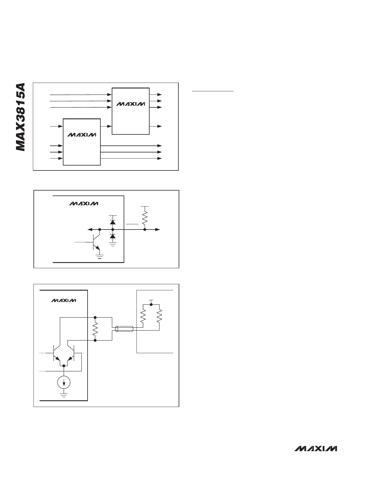
Figure 2. Connection Scheme for MAX3815A in Dual Link
Application
MAX3815A
TO CHIP POWER-
CONTROL CIRCUITRY
VCC
VCC
4.7kΩ
CLKLOS
Figure 3. Simplified CLKLOS Output Circuit Schematic
MAX3815A
RX_OUT+
267Ω
RX_OUT-
+3.3V
50Ω 50Ω
HDM/DVI
RECEIVER
Applications Information
Typical shielded twisted pair (STP), unshielded twisted
pair (UTP), and twin-ax cables exhibit skin-effect losses,
which attenuate the high-frequency spectrum of a TMDS
signal, eventually causing data errors or even closing
the signal eye altogether given a long enough cable. The
MAX3815A recovers the data and opens the signal eye
through compensating equalization.
The basic TMDS interface is composed of four differential
serial links: three links carry serial data up to 2.25Gbps
each, and the fourth is a one-tenth-rate (0.1x) clock that
operates up to 225MHz. TMDS, as with analog nVGA
links, must handle a variety of resolutions and screen
update rates. The actual range of digital serial rates is
roughly 250Mbps to 2.25Gbps. For applications requir-
ing ultra-high resolutions (e.g., QXGA), a “dual-link” DVI
interface is used and is composed of six data links plus
the clock, requiring two MAX3815A ICs with the clock
going to both ICs. See Figure 2.
The MAX3815A can be used to extend any TMDS inter-
face as used under the following trademarked names:
DVI (digital visual interface), DFP™ (digital flat-panel),
PanelLink, ADC™ (Apple display connector), and HDMI
(high-definition multimedia interface).
Loss-of-Clock Signal (CLKLOS) Output
A loss-of-clock signal is indicated by the CLKLOS out-
put. A low level on CLKLOS indicates that the signal
power on the RXC_IN pins has dropped below a thresh-
old. When there is sufficient input voltage to the channel
(typically greater than 100mVP-P differential), CLKLOS is
high. The CLKLOS output is suitable for indicating prob-
lems with the transmission link caused by, for example,
a broken cable, a defective driver, or a lost connection
to the equalizer. Note that the loss-of-clock circuitry is
sensitive to a DC or AC voltage between the RXC_IN
pins. A DC or AC voltage greater than Q30mV (typical) is
sensed as an active clock signal.
12.5mA
Figure 4. Back Termination Circuit
DFP is a trademark of Video Electronics Standards Association (VESA).
ADC is a trademark of Apple Computer, Inc.
8 _______________________________________________________________________________________
Share Link: 