MAX3544 Просмотр технического описания (PDF) - Maxim Integrated
Номер в каталоге
Компоненты Описание
производитель
MAX3544 Datasheet PDF : 20 Pages
| |||
Multiband Digital Television Tuner
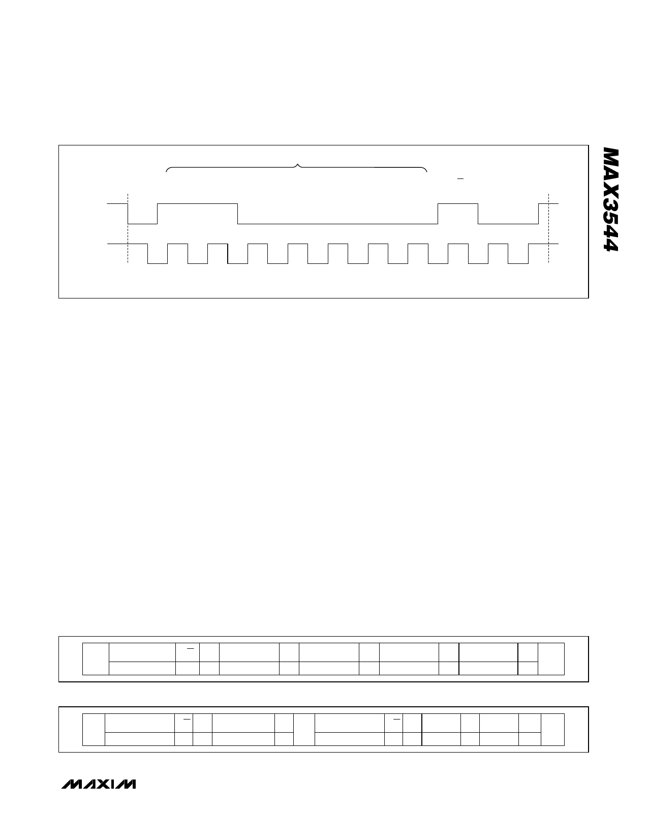
S
SDA
SLAVE ADDRESS
1
1
0
0
0
ADDR2
ADDR1
R/W
ACK
P
SCL
1
2
3
4
5
6
7
8
9
NOTE: TIMING PARAMETERS CONFORM WITH I2C BUS SPECIFICATIONS.
Figure 1. MAX3544 Slave Address Byte. Example shows read address 0x0C1 (ADDR pin grounded).
The MAX3544 continuously awaits a START condition fol-
lowed by its slave address. When the device recognizes
its slave address, it acknowledges by pulling the SDA
line low for one clock period; it is ready to accept or send
data depending on the R/W bit (Figure 1).
Write Cycle
When addressed with a write command, the MAX3544
allows the master to write to a single register or to mul-
tiple successive registers.
A write cycle begins with the bus master issuing a START
condition followed by the 7 slave address bits and a write
bit (R/W = 0). The MAX3544 issues an ACK if the slave
address byte is successfully received. The bus master
must then send to the slave the address of the first reg-
ister it wishes to write to. If the slave acknowledges the
address, the master can then write 1 byte to the register
at the specified address. Data is written beginning with
the most significant bit. The MAX3544 again issues an
ACK if the data is successfully written to the register.
The master can continue to write data to the successive
internal registers with the MAX3544 acknowledging each
successful transfer, or it can terminate transmission by
issuing a STOP condition. The write cycle does not termi-
nate until the master issues a STOP condition.
Figure 2 illustrates an example in which registers 0, 1,
and 2 are written with 0x0E, 0xD8, and 0xE1, respectively.
Read Cycle
A read cycle begins with the bus master issuing a START
condition followed by the 7 slave address bits and a
write bit (R/W = 0). The MAX3544 issues an ACK if the
slave address byte is successfully received. The master
then sends the 8-bit address of the first register that it
wishes to read. The MAX3544 then issues another ACK.
Next, the master must issue a START condition followed
by the 7 slave address bits and a read bit (R/W = 1). The
MAX3544 issues an ACK if it successfully recognizes
its address and begins sending data from the speci-
fied register address starting with the most significant
bit (MSB). Data is clocked out of the MAX3544 on the
rising edge of SCL. On the ninth rising edge of SCL, the
master can issue an ACK and continue reading succes-
sive registers or it can issue a NACK followed by a STOP
condition to terminate transmission. The read cycle does
not terminate until the master issues a STOP condition.
Figure 3 illustrates an example in which registers 0 and
1 are read back.
START
WRITE DEVICE
ADDRESS
R/W
ACK
WRITE REGISTER
ADDRESS
ACK
WRITE DATA TO
REGISTER 0x00
ACK
WRITE DATA TO
REGISTER 0x01
ACK
WRITE DATA TO
REGISTER 0x02
ACK
STOP
11000[ADDR2][ADDR1] 0 —
0x00
—
0x0E
—
0xD8
—
0xE1
—
Figure 2. Example: Write registers 0, 1, and 2 with 0x0E, 0xD8, and 0xE1, respectively.
START
WRITE DEVICE
ADDRESS
R/W
ACK
WRITE 1ST REGISTER
ADDRESS
ACK
START
WRITE DEVICE
ADDRESS
R/W ACK
READ DATA
REG 0
ACK
READ DATA
REG 1
NACK
STOP
110000[ADDR2][ADDR1] 0 —
0x00
—
110000[ADDR2][ADDR1] 1 — D7–D0 — D7–D0 —
Figure 3. Example: Read data from registers 0 and 1.
_______________________________________________________________________________________ 9
Share Link: 