MAX3544 Просмотр технического описания (PDF) - Maxim Integrated
Номер в каталоге
Компоненты Описание
производитель
MAX3544 Datasheet PDF : 20 Pages
| |||
Multiband Digital Television Tuner
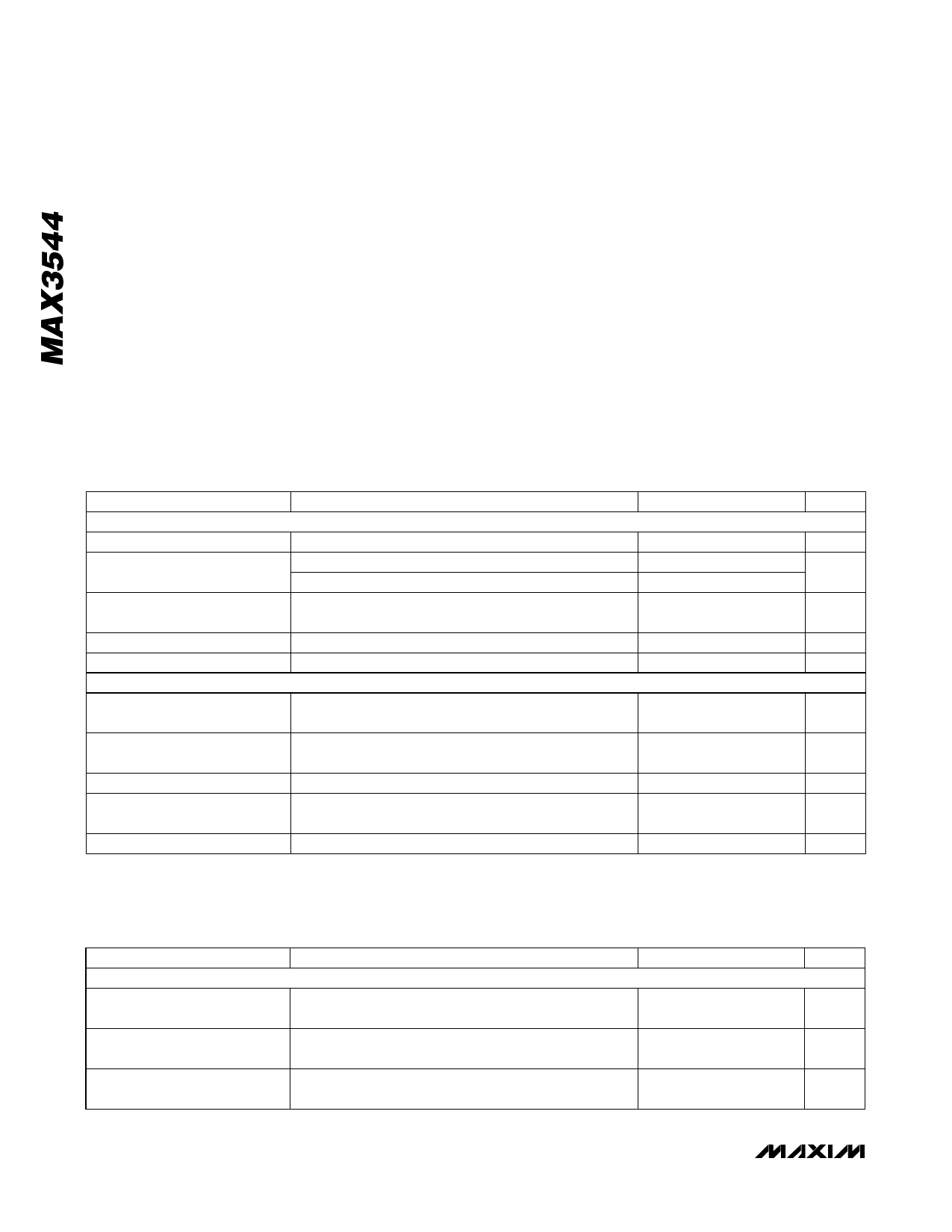
ABSOLUTE MAXIMUM RATINGS
VCC to GND..........................................................-0.3V to +3.6V
RFINL, RFINH, IFIN+, IFIN-, DTVOUT+, DTVOUT-,
IFOUT1A, IFOUT1B.............................. -0.3V to (VCC + 0.3V)
SDA, SCLK, IFAGC, RFVGA.................................-0.3V to +3.6V
Short-Circuit Protection: DTVOUT+, DTVOUT-,
IFOUT1A, IFOUT1B................................................... Indefinite
RF Input Power.............................................................. +10dBm
Continuous Power Dissipation (TA = +70NC)
(derate 35.7mW/NC above +70NC).............................2857mW
Operating Temperature Range.............................. 0NC to +70NC
Junction Temperature......................................................+150NC
Storage Temperature Range............................ -65NC to +165NC
Lead Temperature (soldering, 10s).................................+300NC
Soldering Temperature (reflow).......................................+260NC
Stresses beyond those listed under “Absolute Maximum Ratings” may cause permanent damage to the device. These are stress ratings only, and functional
operation of the device at these or any other conditions beyond those indicated in the operational sections of the specifications is not implied. Exposure to absolute
maximum rating conditions for extended periods may affect device reliability.
DC ELECTRICAL CHARACTERISTICS
(MAX3544 Evaluation Kit, VCC = 3.1V to 3.5V, TA = 0NC to +70NC, registers set according to Table 1. Typical values are at VCC =
3.3V, TA = +25NC, unless otherwise noted.) (Note 1)
PARAMETER
CONDITIONS
MIN TYP MAX UNITS
SUPPLY VOLTAGE AND CURRENT
Supply Voltage
3.1
3.5
V
Supply Current
IF VGA enabled
Standby (REF oscillator on) R08[7] = 1
225 270
mA
5
RF and IF VGC Input
Bias Current
At 0.5V to 3.0V DC
-100 to
+100
FA
RF and IF VGC Control Voltage Maximum gain
3.0
V
RF and IF VGC Control Voltage Minimum gain
0.5
V
SERIAL INTERFACE
Input Logic-Level Low
0.3 x
VCC
V
Input Logic-Level High
0.7 x
VCC
V
Output Logic-Level Low
3mA sink current
0.4
V
Output Logic-Level High
VCC -
0.5V
V
Maximum Clock Rate
400
kHz
AC ELECTRICAL CHARACTERISTICS
(MAX3544 Evaluation Kit, RF center frequency = 666MHz, IF center frequency = 36.15MHz, registers set according to Table 1,
fREF = 16MHz, VRFVGC = VIFVGC = 3.0V, VCC = 3.3V, TA = +25NC, unless otherwise noted.)
PARAMETER
CONDITIONS
OVERALL REQUIREMENTS (RF INPUT TO IF OUTPUT)
RFINL Operating
Frequency Range
Tunable frequency range
MIN TYP MAX UNITS
47
345 MHz
RFINH Operating
Frequency Range
Tunable frequency range
345
862 MHz
Maximum Voltage
Gain to IFOUT1
DVB-T mode (see Table 1)
50
dB
2 _______________________________________________________________________________________
Share Link: 