MAX3544 Просмотр технического описания (PDF) - Maxim Integrated
Номер в каталоге
Компоненты Описание
производитель
MAX3544 Datasheet PDF : 20 Pages
| |||
Multiband Digital Television Tuner
Control Register Description
The MAX3544 includes 18 programmable registers,
two status registers (read only), one register for ROM
readback (read only), and one for Maxim use only. The
programmable registers configure the VCO settings, PLL
settings, detector and AGC settings, state control, bias
adjustments, individual block shutdown, and the track-
ing filter frequency. These programmable registers are
also readable. The read-only registers include two status
registers and a ROM table data register.
Typical bit settings are provided only for user conve-
nience and are not guaranteed at power-up. All registers
must be written no earlier than 100Fs after power-up
or recovery from a brownout event (i.e., when VCC
drops below 1V) to initialize the registers. Then follow
up by rewriting the registers needed for channel/fre-
quency programming (i.e., registers R00–R04). The typi-
cal values listed in Table 3 configure the MAX3544 for
DVB-T reception with 16MHz crystal, 8MHz channel BW,
36.15MHz IF center frequency, differential LC bandpass
filter, and 666MHz RF center frequency.
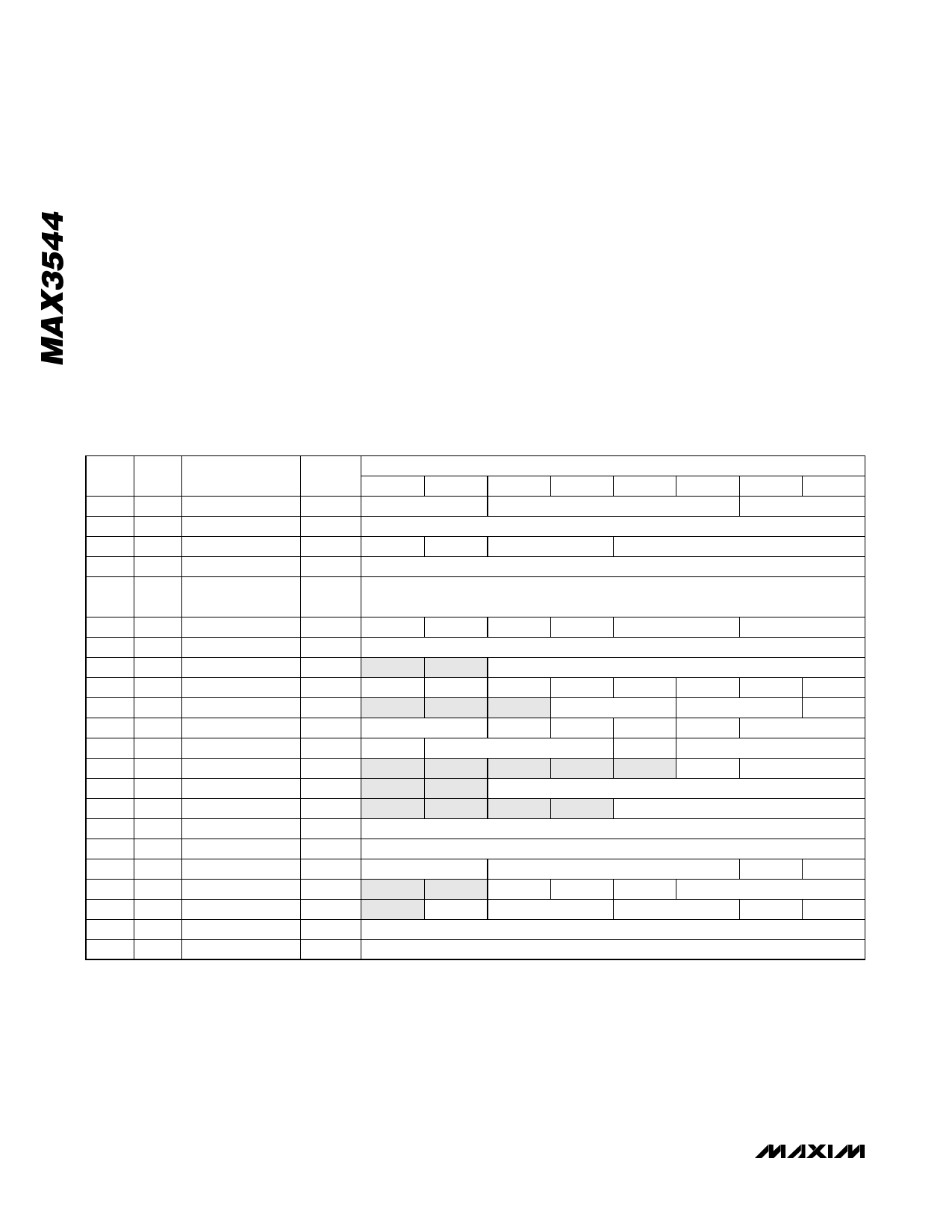
Table 3. Register Configuration
REG REG
REGISTER TYPICAL MSB
BIT LOCATION
LSB
ADDR NAME FUNCTION SETTING 7
6
5
4
3
2
1
0
0x00 R00
VCO
4C
VCO[1:0]
VSUB[3:0]
VDIV[1:0]
0x01 R01
NDIV INT
2B
NINT[7:0]
0x02 R02 NDIV FRAC2
8E
CPS
CP
RDIV[1:0]
F[19:16]
0x03 R03 NDIV FRAC1
26
F[15:8]
0x04 R04
NDIV FRAC0
(VAS Trigger)
66
F[7:0]
0x05 R05 MODE CTRL
D8 LNA2G RFIN RFLPF CHBW
TFB[1:0]
IFSEL[1:0]
0x06 R06
TFS
30
TFS[7:0]
0x07 R07
TFP
12
—
—
TFP[5:0]
0x08 R08 SHUTDOWN
00
STBY SDRF SDMIX SDIF SDIFVG SDPD SDSYN SDVCO
0x09 R09 REF CONFIG
0A
—
—
—
CPLIN[1:0]
ALC[1:0]
XODIV
0x0A R0A VAS CONFIG
17
LFDIV[1:0]
VASS VAS
ADL
ADE
LTC[1:0]
0x0B R0B PWRDET CFG1
43
DWPD
WPDA[2:0]
DNPD
NPDA[2:0]
0x0C R0C PWRDET CFG2
01
—
—
—
—
— PULLUP
RFIFD[1:0]
0x0D R0D FILT CF ADJ
ROM
—
—
CFSET[5:0]
0x0E R0E
ROM ADDR
00
—
—
—
—
ROMA[3:0]
0x0F R0F
IRHR
ROM
IRHR[7:0]
0x10 R10 ROM READBACK RO
ROMR[7:0]
0x11 R11 VAS STATUS
RO
VVCO[1:0]
VVSB[3:0]
VASA VASE
0x12 R12 GEN STATUS
RO
—
—
VCP
TRIM
POR
VCOADC[2:0]
0x13 R13
BIAS ADJ
56
—
MIXGM
LNA2B[1:0]
MIXB[1:0]
FILTB IFVGAB
0x14 R14
TEST1
40
RESERVED
0x15 R15 ROM WRITE DATA 00
ROMW[7:0]
Note: Registers should be written in the order of ascending addresses. When changing frequency, write R00 to R07 in order of
ascending addresses to ensure proper VCO setup.
10 �������������������������������������������������������������������������������������
Share Link: 