MAX3344E –Я—А–Њ—Б–Љ–Њ—В—А —В–µ—Е–љ–Є—З–µ—Б–Ї–Њ–≥–Њ –Њ–њ–Є—Б–∞–љ–Є—П (PDF) - Maxim Integrated
–Э–Њ–Љ–µ—А –≤ –Ї–∞—В–∞–ї–Њ–≥–µ
–Ъ–Њ–Љ–њ–Њ–љ–µ–љ—В—Л –Ю–њ–Є—Б–∞–љ–Є–µ
–њ—А–Њ–Є–Ј–≤–Њ–і–Є—В–µ–ї—М
MAX3344E Datasheet PDF : 15 Pages
| |||
±15kV ESD-Protected USB Transceivers
in UCSP with USB Detect
ABSOLUTE MAXIMUM RATINGS
(All voltages refer to GND, unless otherwise noted.)
Supply Voltage (VCC) ...............................................-0.3V to +6V
Output of Internal Regulator (VTRM) ..........-0.3V to (VCC + 0.3V)
Input Voltage (D+, D-) ..............................................-0.3V to +6V
System Supply Voltage (VL) .....................................-0.3V to +6V
RCV, SUSP, VMO, MODE, VPO, OE, VMI,
VPI, USB_DET, ENUM...............................-0.3V to (VL + 0.3V)
Short-Circuit Current (D+, D-) to VCC or
GND (Note 1) .........................................................Continuous
Note 1: External 23.7вД¶ resistors connected to D+ and D-.
Maximum Continuous Current (all other pins) ..................±15mA
Continuous Power Dissipation (TA = +70°C)
16-Pin TSSOP (derate 9.4mW/°C above +70°C)...754mW (U16-2)
4 вЬХ 4 UCSP (derate 8.2mW/¬∞C above +70¬∞C) ...659mW (B16-1)
Operating Temperature Range ...........................-40°C to +85°C
Junction Temperature ......................................................+150°C
Storage Temperature Range .............................-65°C to +150°C
Lead Temperature (soldering, 10s) .................................+300°C
Bump Temperature (soldering) Reflow............................+235°C
Stresses beyond those listed under вАЬAbsolute Maximum RatingsвАЭ may cause permanent damage to the device. These are stress ratings only, and functional
operation of the device at these or any other conditions beyond those indicated in the operational sections of the specifications is not implied. Exposure to
absolute maximum rating conditions for extended periods may affect device reliability.
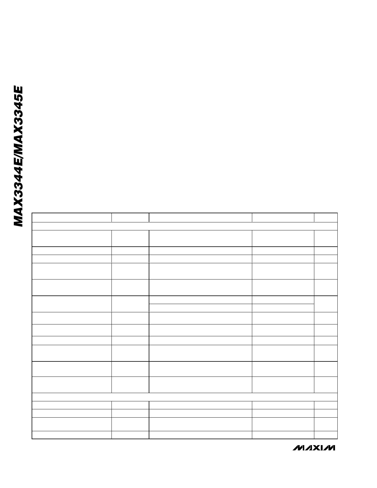
ELECTRICAL CHARACTERISTICS
(VCC = 4V to 5.5V bypassed with 1µF to GND, GND = 0, VL = 1.65V to 3.6V, ENUM = VL, TA = TMIN to TMAX, unless otherwise
noted. Typical values are at VCC = 5V, VL = 2.5V, TA = +25°C.) (Note 2)
PARAMETER
SYMBOL
SUPPLY INPUTS (VCC, VTRM, VL)
Regulated Supply Voltage
Output
VVTRM
VCC Input Range
VCC
VL Input Range
VL
Operating VCC Supply Current
IVCC
Operating VL Supply Current
Full-Speed Idle and SE0 Supply
Current
Static VL Supply Current
IVL
IVCC(IDLE)
IVL(STATIC)
CONDITIONS
Internal regulator
Full-speed transmitting/receiving at
12Mbps, CL = 50pF on D+ and D-
Full-speed transmitting/receiving at
12Mbps
Full-speed idle: VD+ > 2.7V, VD- < 0.3V
SE0: VD+ < 0.3V, VD- < 0.3V
Full-speed idle, SE0, or suspend mode
MIN TYP MAX UNITS
3.0
3.3
3.6
V
4.0
5.5
V
1.65
3.60
V
10
mA
8
mA
340 450
µA
390 500
12.5
µA
Suspend Supply Current
Disable-Mode Supply Current
D+/D- Disable-Mode
Load Current
Sharing-Mode VL Supply
Current
D+/D- Sharing-Mode
Load Current
LOGIC-SIDE I/O
Input High Voltage
Input Low Voltage
Output-Voltage High
Output-Voltage Low
IVCC(SUSP)
IVCC(DIS)
SUSP = OE = high
VL = GND or open
ID_(DIS) VL = GND or open, VD_ = 0 or +5.5V
IVL(SHARING)
VCC = GND or open, OE = low, SUSP =
high
ID_(SHARING) VCC = GND or open, VD_ = 0 or +5.5V
VIH
SUSP, MODE, ENUM, OE, VMO, VPO
2/3 x VL
VIL
SUSP, MODE, ENUM, OE, VMO, VPO
VOH
VPI, VMI, RCV, USB_DET; ISOURCE =
2mA
VL - 0.4
VOL
VPI, VMI, RCV, USB_DET; ISINK = -2mA
40
µA
20
µA
5
µA
20
µA
20
µA
V
0.4
V
V
0.4
V
2 _______________________________________________________________________________________
Share Link: 