MAX3272 Просмотр технического описания (PDF) - Maxim Integrated
Номер в каталоге
Компоненты Описание
производитель
MAX3272 Datasheet PDF : 14 Pages
| |||
+3.3V, 2.5Gbps Low-Power
Limiting Amplifiers
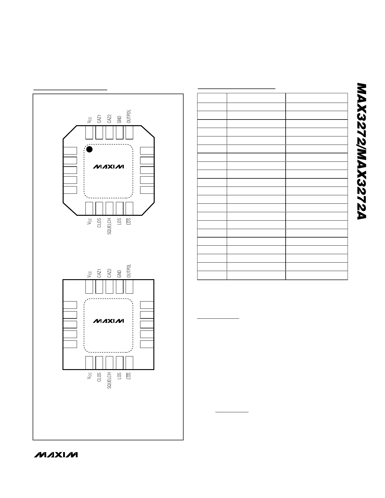
Pin Configuration
TOP VIEW
GND 1
IN+ 2
IN- 3
GND 4
TH 5
20 19 18 17 16
MAX3272/
MAX3272A
15 VCC
14 OUT+
13 OUT-
12 VCC
11 LEVEL
6 7 8 9 10
QFN*
NOTE: EXPOSED PAD MUST BE CONNECTED TO SUPPLY GROUND.
GND 1
IN+ 2
IN- 3
GND 4
TH 5
20 19 18 17 16
+
MAX3272A
15 VCC
14 OUT+
13 OUT-
12 VCC
11 LEVEL
6 7 8 9 10
THIN QFN*
NOTE: EXPOSED PAD MUST BE CONNECTED TO SUPPLY GROUND.
Pad Coordinates
PAD
NAME
COORDINATES (µm)
1
GND
47, 836
2
IN+
47, 603
3
IN-
47, 425
4
GND
47, 237
5
TH
47, 47
6
VCC
7
CLOS
255, -154
436, -154
8
SQUELCH
645, -154
9
LOS
10
LOS
850, -154
1063, -154
11
LEVEL
1331, 37
12
VCC
13
OUT-
1331, 212
1331, 421
14
OUT+
1331, 573
15
VCC
16
OUTPOL
1331, 780
1119, 1042
17
GND
957, 1042
18
CAZ2
773, 1042
19
CAZ1
583, 1042
20
N.C.
422, 1042
21
VCC
268, 1042
Coordinates are for the center of the pad.
Coordinate 0, 0 is the lower left corner of the passivation open-
ing for pad 5.
Applications Information
Optical Hysteresis
In an optical receiver, the electrical power change at the
limiting amplifier is 2 times the optical power change.
As an example, if a receiver’s optical input power (x)
increases by a factor of two, and the preamplifier is lin-
ear, then the voltage input to the limiting amplifier also
increases by a factor of two.
The optical power change is 10log(2x / x) = 10log(2) =
+3dB.
At the limiting amplifier, the electrical power change is:
( ) 10log
2VIN 2 / RIN
VIN2 / RIN
= 10log(22 ) = 20log(2) =
+ 6dB
The MAX3272 typical voltage hysteresis is 3.3dB. This
provides an optical hysteresis of 1.65dB.
_______________________________________________________________________________________ 9
Share Link: 