MAX1763EUE(2001) Просмотр технического описания (PDF) - Maxim Integrated
Номер в каталоге
Компоненты Описание
производитель
MAX1763EUE Datasheet PDF : 16 Pages
| |||
1.5A, Low-Noise, 1MHz, Step-Up
DC-DC Converter
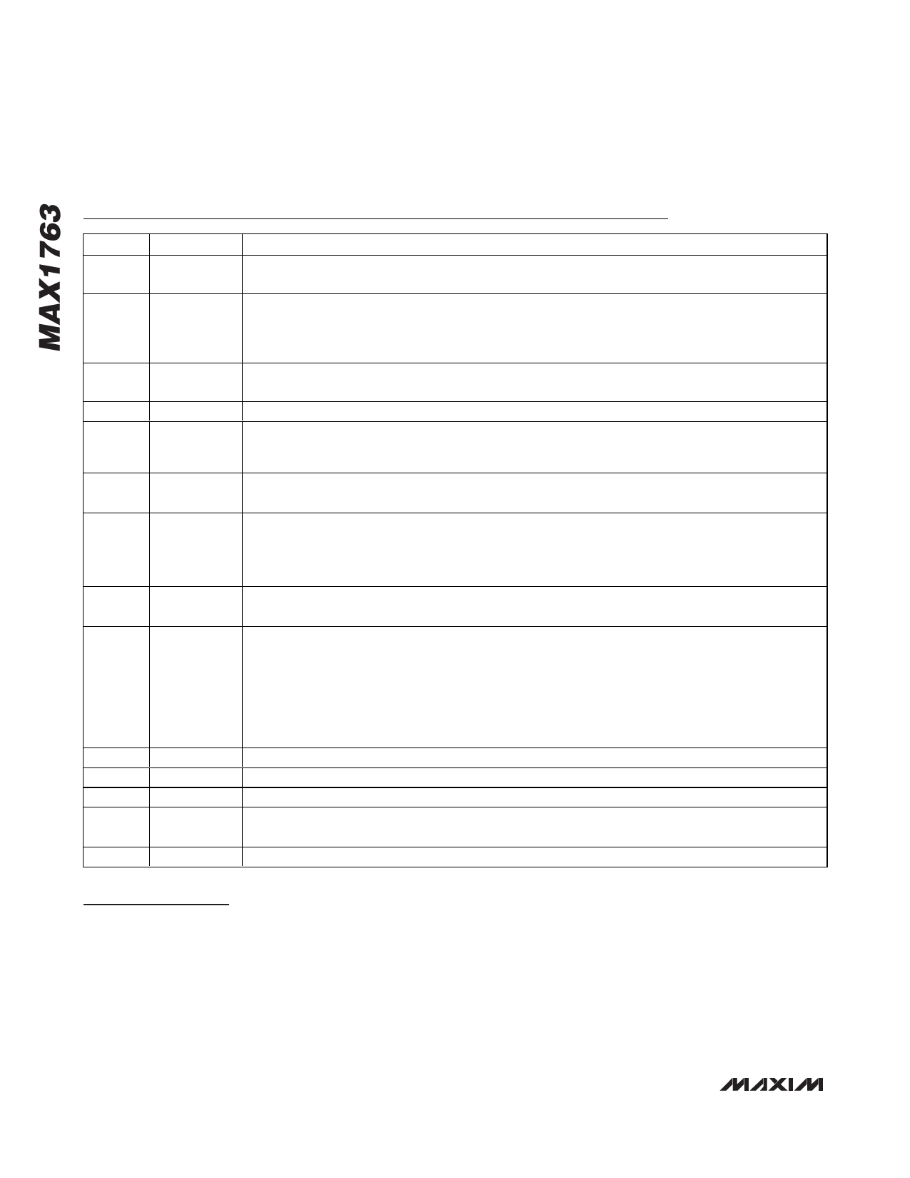
PIN
1
2
3
4
5
6
7
8
9
10, 12
11, 14
13, 15
16
NAME
ONA
ISET
REF
GND
FB
OUT
AIN
AO
CLK/SEL
PGND
LX
POUT
ONB
Pin Description
FUNCTION
On Control Input. When ONA = high or ONB = low, the IC turns on. Connect ONA to OUT for normal
operation (Table 3).
N-Channel Current Limit Control. For maximum current limit, connect to REF. To reduce current,
supply a voltage between REF and GND by means of a resistive voltage-divider. If soft-start is
desired, connect a capacitor from ISET to GND. When ONA = low and ONB = high, or VREF < 80% of
nominal value, an on-chip switched resistor (100kΩ typ) discharges this pin to GND.
1.250V Voltage Reference Bypass Pin. Connect a 0.22µF ceramic bypass capacitor to GND. Up to
50µA of external REF load current is allowed.
Ground. Connect to PGND with short trace.
DC-DC Converter Feedback Input. To set fixed output voltage of +3.3V, connect FB to ground. For
adjustable output of 2.5V to 5.5V, connect to a resistive divider placed from OUT to GND. FB set
point is 1.245V (Figure 6).
IC Power, Supplied from the Output. Bypass to GND with a 1.0µF ceramic capacitor, and connect to
POUT with a series 4.7Ω resistor (Figure 2).
Gain-Block Input. The nominal transconductance from AIN to AO is 10mS. An external P-channel
pass device can be used to build a linear regulator. The gain block can also be used as a low-battery
comparator with a threshold of 0.938V. The gain block and its associated quiescent current are
disabled by connecting AIN to OUT.
Gain-Block Output. This open-drain N-channel output sinks current when VAIN < (0.75)(VREF). AO is
high-Z when the device is shut down, or when AIN = OUT.
Clock Input for the DC-DC Converter. Also serves to program the operating mode of the switcher as
follows:
CLK/SEL = LO: Normal; operates at a fixed frequency, automatically switching to low-power mode if
load is minimized.
CLK/SEL = HI: Forced PWM mode; operates in low-noise, constant-frequency mode at all loads.
CLK/SEL = Clocked: Forced PWM mode with the internal oscillator synchronized to CLK in 500kHz
to 1200kHz range.
Source of N-Channel Power MOSFET Switch. Connect both PGND pins together close to the device.
Inductor Connection. Connect the LX pins together close to the device.
Power Output. P-channel synchronous rectifier source.
Off Control Input. When ONB = high and ONA = low, the IC is off. Connect ONB to GND for normal
operation (Table 3).
Detailed Description
The MAX1763 is a highly-efficient, low-noise power
supply for portable RF and hand-held instruments. It
combines a boost switching regulator, N-channel
power MOSFET, P-channel synchronous rectifier, preci-
sion reference, shutdown control, and a versatile gain
block (Figure 1).
The DC-DC converter boosts a one-cell to three-cell
battery voltage input to a fixed 3.3V or adjustable volt-
age between 2.5V and 5.5V. An external Schottky
diode is required for output voltages greater than 4V.
The MAX1763 guarantees startup with an input voltage
as low as 1.1V and remains operational down to an
input of just 0.7V. It is optimized for use in cellular
phones and other applications requiring low noise and
low quiescent current for maximum battery life. It fea-
tures constant-frequency (1MHz), low-noise PWM oper-
ation with up to 1.5A output capability. A CLK input
allows frequency synchronization to control the output
8 _______________________________________________________________________________________
Share Link: 