IDT72V36100L6PFG Просмотр технического описания (PDF) - Integrated Device Technology
Номер в каталоге
Компоненты Описание
производитель
IDT72V36100L6PFG Datasheet PDF : 48 Pages
| |||
IDT72V36100/72V36110 3.3V HIGH DENSITY SUPERSYNC IITM 36-BIT FIFO
65,536 x 36 and 131,072 x 36
COMMERCIAL AND INDUSTRIAL
TEMPERATURE RANGES
AC TEST CONDITIONS
Input Pulse Levels
Input Rise/Fall Times
Input Timing Reference Levels
Output Reference Levels
Output Load for tCLK = 10ns, 15 ns
Output Load for tCLK = 6ns, 7.5ns
GND to 3.0V
3ns(1)
1.5V
1.5V
See Figure 2a
See Figure 2b & 2c
NOTE:
1. For 166MHz and 133MHz operation input rise/fall times are 1.5ns.
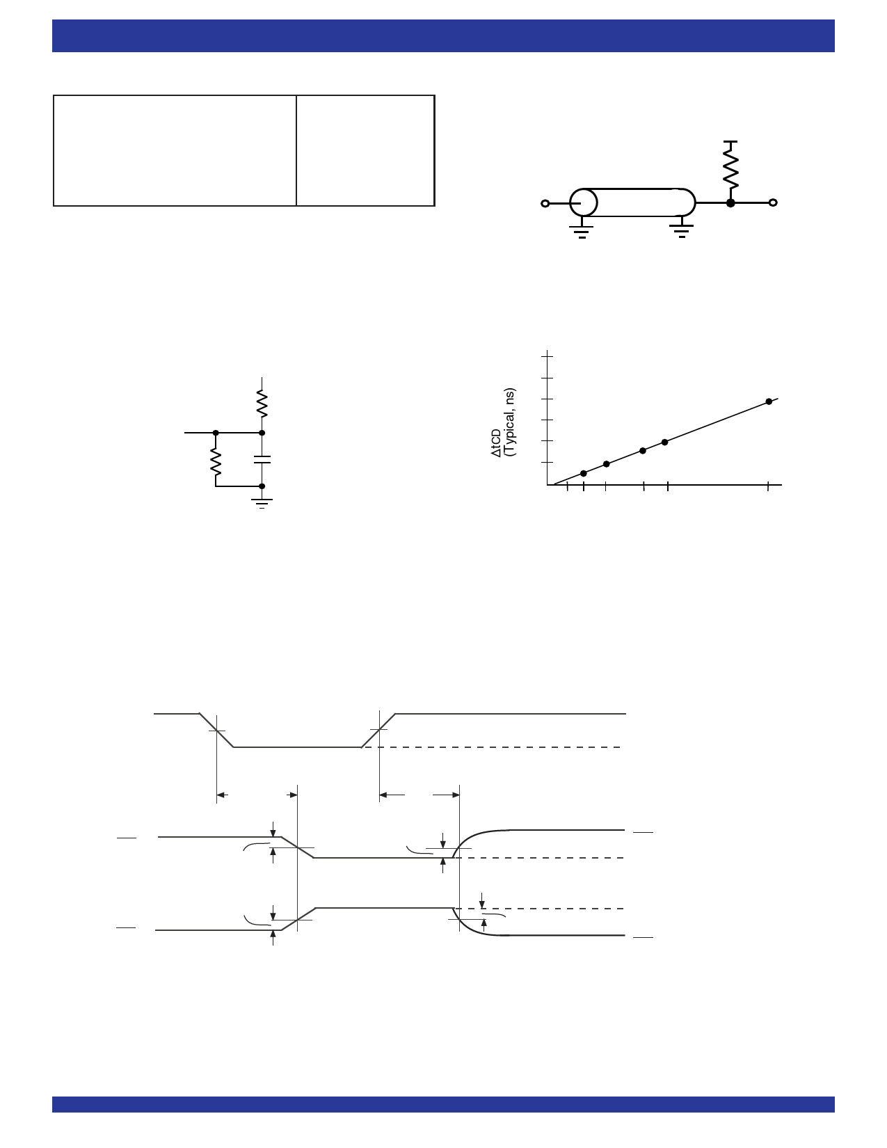
AC TEST LOADS - 6ns, 7.5ns Speed Grade
1.5V
50Ω
I/O
Z0 = 50Ω
6117 drw04a
Figure 2b. AC Test Load
AC TEST LOADS - 10ns, 15ns Speed Grades
D.U.T.
510Ω
3.3V
330Ω
30pF*
6117 drw04
Figure 2a. Output Load
* Includes jig and scope capacitances.
6
5
4
3
2
1
20 30 50 80 100
Capacitance (pF)
200
6117 drw04b
Figure 2c. Lumped Capacitive Load, Typical Derating
OUTPUT ENABLE & DISABLE TIMING
Output
Enable
OE
Output
Disable
Output VCC
Normally
LOW
2
Output
Normally VCC
HIGH 2
tOE & tOLZ
100mV
100mV
tOHZ
100mV
100mV
VIH
VIL
VCC
2
VOL
VOH
VCC
2
6117 drw04c
11
Share Link: 