HT48R10A-1 Просмотр технического описания (PDF) - Holtek Semiconductor
Номер в каталоге
Компоненты Описание
производитель
HT48R10A-1 Datasheet PDF : 38 Pages
| |||
HT48R10A-1/HT48C10-1
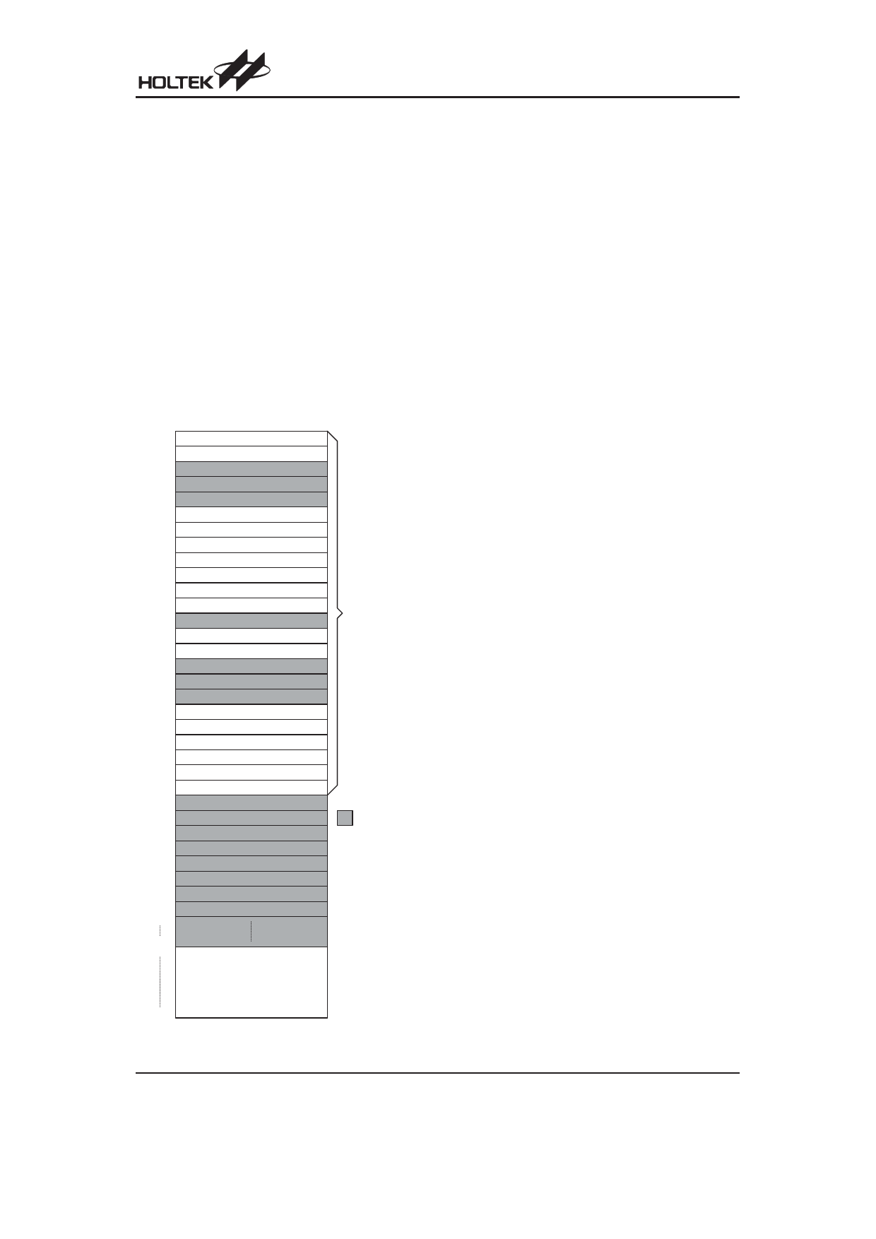
Data Memory - RAM
The data memory is designed with 81´8 bits. The data
memory is divided into two functional groups: special
function registers and general purpose data memory
(64´8). Most are read/write, but some are read only.
The special function registers include the indirect ad-
dressing register (00H), timer/event counter
(TMR;0DH), timer/event counter control register
(TMRC;0EH), program counter lower-order byte regis-
ter (PCL;06H), memory pointer register (MP;01H), ac-
cumulator (ACC;05H), table pointer (TBLP;07H), table
higher-order byte register (TBLH;08H), status register
(STATUS;0AH), interrupt control register (INTC;0BH),
Watchdog Timer option setting register (WDTS;09H),
I/O registers (PA;12H, PB;14H, PC;16H) and I/O control
registers (PAC;13H, PBC;15H, PCC;17H). The remain-
ing space before the 40H is reserved for future ex-
00H
In d ir e c t A d d r e s s in g R e g is te r
01H
MP
02H
03H
04H
05H
ACC
06H
PCL
07H
TB LP
08H
TB LH
09H
W D TS
0A H
STATU S
0B H
IN T C
0C H
S p e c ia l P u r p o s e
D ATA M EM O R Y
0D H
TM R
0E H
TM R C
0FH
10H
11H
12H
PA
13H
PAC
14H
PB
15H
PBC
16H
PC
17H
PCC
18H
19H
:U nused
1A H
R e a d a s "0 0 "
1B H
1C H
1D H
1E H
1FH
20H
3FH
40H
G e n e ra l P u rp o s e
D ATA M EM O R Y
(6 4 B y te s )
7FH
RAM Mapping
panded usage and reading these locations will get
²00H². The general purpose data memory, addressed
from 40H to 7FH, is used for data and control informa-
tion under instruction commands.
All of the data memory areas can handle arithmetic,
logic, increment, decrement and rotate operations di-
rectly. Except for some dedicated bits, each bit in the
data memory can be set and reset by ²SET [m].i² and
²CLR [m].i². They are also indirectly accessible through
memory pointer register (MP;01H).
Indirect Addressing Register
Location 00H is an indirect addressing register that is
not physically implemented. Any read/write operation of
[00H] accesses data memory pointed to by MP (01H).
Reading location 00H itself indirectly will return the re-
sult 00H. Writing indirectly results in no operation.
The memory pointer register MP (01H) is a 7-bit register.
The bit 7 of MP is undefined and reading will return the re-
sult ²1². Any writing operation to MP will only transfer the
lower 7-bit data to MP.
Accumulator
The accumulator is closely related to ALU operations. It
is also mapped to location 05H of the data memory and
can carry out immediate data operations. The data
movement between two data memory locations must
pass through the accumulator.
Arithmetic and Logic Unit - ALU
This circuit performs 8-bit arithmetic and logic opera-
tions. The ALU provides the following functions:
· Arithmetic operations (ADD, ADC, SUB, SBC, DAA)
· Logic operations (AND, OR, XOR, CPL)
· Rotation (RL, RR, RLC, RRC)
· Increment and Decrement (INC, DEC)
· Branch decision (SZ, SNZ, SIZ, SDZ ....)
The ALU not only saves the results of a data operation
but also changes the status register.
Status Register - STATUS
This 8-bit register (0AH) contains the zero flag (Z), carry
flag (C), auxiliary carry flag (AC), overflow flag (OV),
power down flag (PDF), and watchdog time-out flag
(TO). It also records the status information and controls
the operation sequence.
With the exception of the TO and PDF flags, bits in
the status register can be altered by instructions like
most other registers. Any data written into the status
register will not change the TO or PDF flag. In addi-
tion operations related to the status register may give
different results from those intended. The TO flag
can be affected only by system power-up, a WDT
time-out or executing the ²CLR WDT² or ²HALT² in-
struction. The PDF flag can be affected only by exe-
Rev. 1.90
8
November 4, 2005
Share Link: 