CA3130A Просмотр технического описания (PDF) - Intersil
Номер в каталоге
Компоненты Описание
производитель
CA3130A Datasheet PDF : 17 Pages
| |||
CA3130, CA3130A
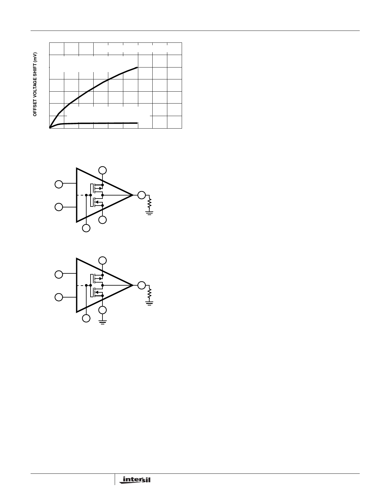
o
7
TA = 125oC FOR TO-5 PACKAGES
6
DIFFERENTIAL DC VOLTAGE
5
(ACROSS TERMINALS 2 AND 3) = 2V
OUTPUT STAGE TOGGLED
4
3
2
DIFFERENTIAL DC VOLTAGE
1
(ACROSS TERMINALS 2 AND 3) = 0V
OUTPUT VOLTAGE = V+ / 2
0
0 500 1000 1500 2000 2500 3000 3500 4000
TIME (HOURS)
FIGURE 5. TYPICAL INCREMENTAL OFFSET-VOLTAGE
SHIFT vs OPERATING LIFE
V+
7
CA3130
3
+
Q8
Q12
2
-
6
RL
4
8
V-
FIGURE 6A. DUAL POWER SUPPLY OPERATION
7 V+
CA3130
3
+
Q8
Q12
2
-
4
8
6
RL
FIGURE 6B. SINGLE POWER SUPPLY OPERATION
FIGURE 6. CA3130 OUTPUT STAGE IN DUAL AND SINGLE
POWER SUPPLY OPERATION
Power-Supply Considerations
Because the CA3130 is very useful in single-supply
applications, it is pertinent to review some considerations
relating to power-supply current consumption under both
single-and dual-supply service. Figures 6A and 6B show the
CA3130 connected for both dual-and single-supply
operation.
Dual-supply Operation: When the output voltage at Terminal
6 is 0V, the currents supplied by the two power supplies are
equal. When the gate terminals of Q8 and Q12 are driven
increasingly positive with respect to ground, current flow
through Q12 (from the negative supply) to the load is
7
increased and current flow through Q8 (from the positive
supply) decreases correspondingly. When the gate terminals
of Q8 and Q12 are driven increasingly negative with respect
to ground, current flow through Q8 is increased and current
flow through Q12 is decreased accordingly.
Single-supply Operation: Initially, let it be assumed that the
value of RL is very high (or disconnected), and that the input-
terminal bias (Terminals 2 and 3) is such that the output
terminal (No. 6) voltage is at V+/2, i.e., the voltage drops
across Q8 and Q12 are of equal magnitude. Figure 20 shows
typical quiescent supply-current vs supply-voltage for the
CA3130 operated under these conditions. Since the output
stage is operating as a Class A amplifier, the supply-current
will remain constant under dynamic operating conditions as
long as the transistors are operated in the linear portion of
their voltage-transfer characteristics (see Figure 2). If either
Q8 or Q12 are swung out of their linear regions toward cut-off
(a non-linear region), there will be a corresponding reduction
in supply-current. In the extreme case, e.g., with Terminal 8
swung down to ground potential (or tied to ground), NMOS
transistor Q12 is completely cut off and the supply-current to
series-connected transistors Q8, Q12 goes essentially to zero.
The two preceding stages in the CA3130, however, continue
to draw modest supply-current (see the lower curve in Figure
20) even though the output stage is strobed off. Figure 6A
shows a dual-supply arrangement for the output stage that
can also be strobed off, assuming RL = ∞ by pulling the
potential of Terminal 8 down to that of Terminal 4.
Let it now be assumed that a load-resistance of nominal
value (e.g., 2kΩ) is connected between Terminal 6 and
ground in the circuit of Figure 6B. Let it be assumed again
that the input-terminal bias (Terminals 2 and 3) is such that
the output terminal (No. 6) voltage is at V+/2. Since PMOS
transistor Q8 must now supply quiescent current to both RL
and transistor Q12, it should be apparent that under these
conditions the supply-current must increase as an inverse
function of the RL magnitude. Figure 22 shows the voltage-
drop across PMOS transistor Q8 as a function of load
current at several supply voltages. Figure 2 shows the
voltage-transfer characteristics of the output stage for
several values of load resistance.
Wideband Noise
From the standpoint of low-noise performance
considerations, the use of the CA3130 is most advantageous
in applications where in the source resistance of the input
signal is on the order of 1MΩ or more. In this case, the total
input-referred noise voltage is typically only 23µV when the
test-circuit amplifier of Figure 7 is operated at a total supply
voltage of 15V. This value of total input-referred noise
remains essentially constant, even though the value of
source resistance is raised by an order of magnitude. This
characteristic is due to the fact that reactance of the input
capacitance becomes a significant factor in shunting the
source resistance. It should be noted, however, that for
Share Link: 