CA3130A Просмотр технического описания (PDF) - Intersil
Номер в каталоге
Компоненты Описание
производитель
CA3130A Datasheet PDF : 17 Pages
| |||
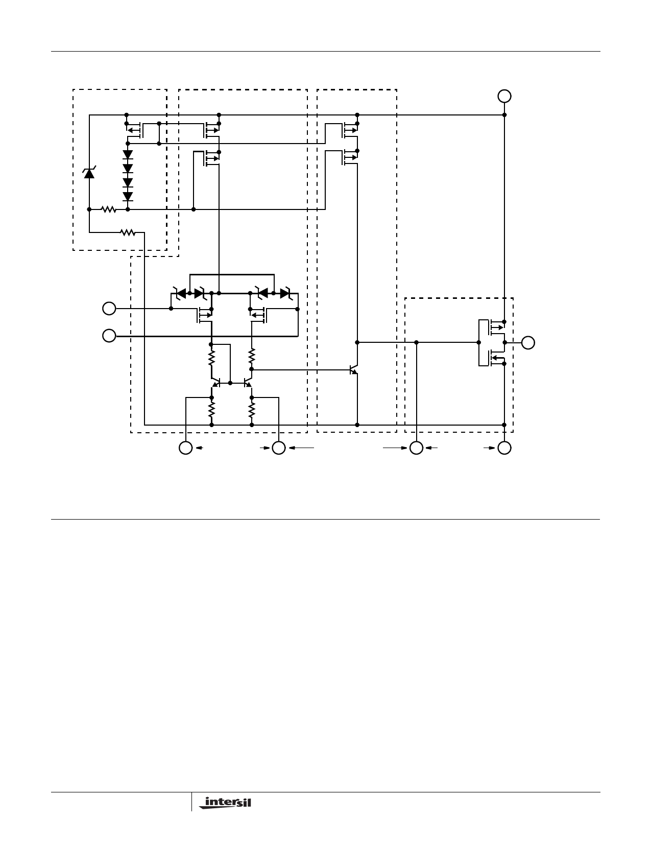
CA3130, CA3130A
Schematic Diagram
BIAS CIRCUIT
CURRENT SOURCE FOR
Q6 AND Q7
Q1
D1
Z1
D2
8.3V
D3
R1
D4
40kΩ R2
5kΩ
Q2
Q4
NON-INV.
INPUT
3+
INV.-INPUT
2-
INPUT STAGE
D5 D6
(NOTE 5) D7 D8
Q6
Q7
R3
R4
1kΩ
1kΩ
Q9 Q10
R5
R6
1kΩ
1kΩ
“CURRENT SOURCE
LOAD” FOR Q11
Q3
Q5
SECOND
STAGE
Q11
OUTPUT
STAGE
7 V+
Q8
OUTPUT
6
Q12
5 OFFSET NULL 1
COMPENSATION
NOTE:
5. Diodes D5 through D8 provide gate-oxide protection for MOSFET input stage.
8
STROBING
4 V-
Application Information
Circuit Description
Figure 1 is a block diagram of the CA3130 Series CMOS
Operational Amplifiers. The input terminals may be operated
down to 0.5V below the negative supply rail, and the output
can be swung very close to either supply rail in many
applications. Consequently, the CA3130 Series circuits are
ideal for single-supply operation. Three Class A amplifier
stages, having the individual gain capability and current
consumption shown in Figure 1, provide the total gain of the
CA3130. A biasing circuit provides two potentials for
common use in the first and second stages.
Terminal 8 can be used both for phase compensation and to
strobe the output stage into quiescence. When Terminal 8 is
tied to the negative supply rail (Terminal 4) by mechanical or
electrical means, the output potential at Terminal 6
essentially rises to the positive supply-rail potential at
Terminal 7. This condition of essentially zero current drain in
4
the output stage under the strobed “OFF” condition can only
be achieved when the ohmic load resistance presented to
the amplifier is very high (e.g.,when the amplifier output is
used to drive CMOS digital circuits in Comparator
applications).
Input Stage
The circuit of the CA3130 is shown in the schematic diagram.
It consists of a differential-input stage using PMOS field-effect
transistors (Q6, Q7) working into a mirror-pair of bipolar
transistors (Q9, Q10) functioning as load resistors together
with resistors R3 through R6.
The mirror-pair transistors also function as a differential-to-
single-ended converter to provide base drive to the second-
stage bipolar transistor (Q11). Offset nulling, when desired,
can be effected by connecting a 100,000Ω potentiometer
across Terminals 1 and 5 and the potentiometer slider arm to
Terminal 4.
Share Link: 