GT28F400B3B150 Просмотр технического описания (PDF) - Intel
Номер в каталоге
Компоненты Описание
производитель
GT28F400B3B150 Datasheet PDF : 49 Pages
| |||
SMART 3 ADVANCED BOOT BLOCK–WORD-WIDE
E
VCCQ
0.0
INPUT
VCCQ
2
TEST POINTS
VCCQ OUTPUT
2
0580_11
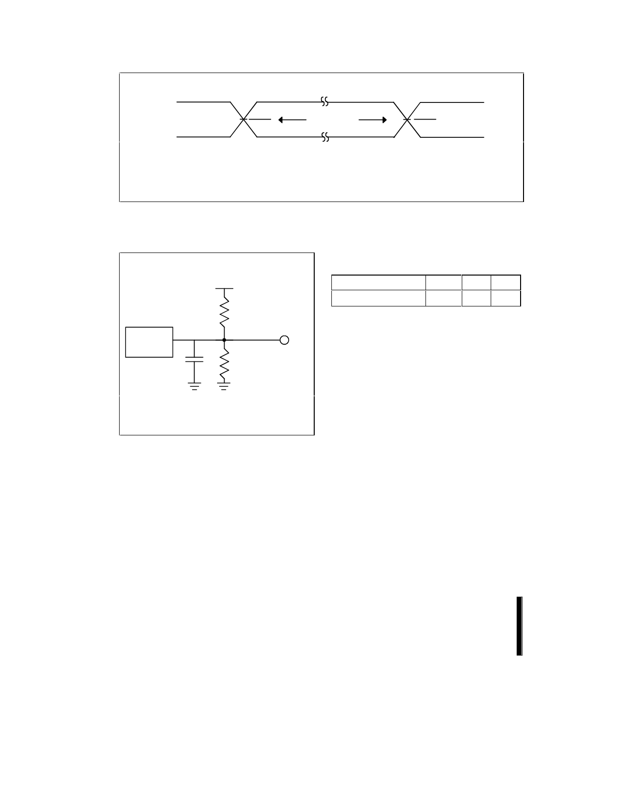
NOTE:
AC test inputs are driven at VCCQ for a logic “1” and 0.0V for a logic “0.” Input timing begins, and output timing ends, at VCCQ/2.
Input rise and fall times (10%–90%) <10 ns. For worst case speed conditions VCCQ = 1.8V.
Figure 13. 1.8V—2.2V Input Range and Measurement Points
Device
under
Test
VCCQ
R1
CL
R2
Test Configuration Component Values for Worst
Case Speed Conditions
Test Configuration
1.8V Standard Test
CL (pF) R1 (Ω) R2 (Ω)
50 16.7K 16.7K
NOTE:
CL includes jig capacitance.
Out
NOTE:
See table for component values.
Figure 14. Test Configuration
0580_12
38
PRELIMINARY
Share Link: 