AD809BRZ Просмотр технического описания (PDF) - Analog Devices
Номер в каталоге
Компоненты Описание
производитель
AD809BRZ Datasheet PDF : 8 Pages
| |||
AD809
USING THE AD809
Ground Planes
Use of one ground plane for connections to both analog and
digital grounds is recommended.
Power Supply Connections
Use of a 10 µF capacitor between VCC and ground is recom-
mended. Care should be taken to isolate the +5 V power trace
to VCC2 (Pin 3). The VCC2 pin is used inside the device to pro-
vide the CLKOUT/CLKOUTN signals.
Use of a trace connecting Pin 14 and Pin 6 (AVCC2 and VCC1
respectively) is recommended. Use of 0.1 µF capacitors between
IC power supply and ground is recommended. Power supply
decoupling should take place as close to the IC as possible.
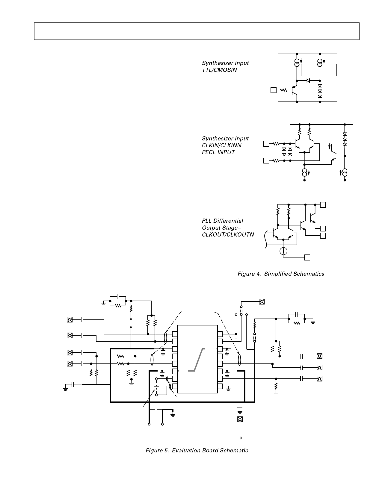
Refer to the schematic, Figure 5, for advised connections.
Transmission Lines
Use of 50 Ω transmission lines are recommended for PECL
inputs.
Terminations
Termination resistors should be used for PECL input signals.
Metal, thick film, 1% tolerance resistors are recommended.
Termination resistors for the PECL input signals should be
placed as close as possible to the PECL input pins.
Connections from the power supply to load resistors for input
and output signals should be individual, not daisy chained. This
will avoid crosstalk on these signals.
Loop Damping Capacitor, CD
A ceramic capacitor may be used for the loop damping capaci-
tor. A 22 nF capacitor provides a damping factor of 10.
Synthesizer Input
TTL/CMOSIN
Synthesizer Input
CLKIN/CLKINN
PECL INPUT
PLL Differential
Output Stage–
CLKOUT/CLKOUTN
500Ω
VCC1
2*ITTL
80µA
OR
0µA
2*ITTL
80µA
OR
0µA
VEE
500Ω
7.5kΩ
VCC1
7.5kΩ
ITTL
500Ω
40µA
VEE
40µA
460Ω
460Ω
VCC2
DIFFERENTIAL
OUTPUT
2.6mA
VEE
Figure 4. Simplified Schematics
J1 C2 0.1µF
ECL INN
J2 C3 0.1µF
ECL IN
J3 C4 0.1µF
CLKOUTN
J4 C5 0.1µF
CLKOUT
R3
C6 100Ω
0.1µF
C1
0.1µF
R6
3.65kΩ
R5
301Ω
JUMPER
R1
W2 49.9Ω
R7 100Ω
R8 100Ω
R4
100Ω
R11
154Ω
R12
154Ω
R2
49.9Ω
50Ω STRIP LINE
EQUAL LENGTH
16-PIN SOIC
SOLDERED TO BOARD
JUMPER
W1
GND
AD809
1 PECLINN
VEE 16
2 PECLIN
MUX 15
C7 3 VCC2
AVCC2 14
C9
4 CLKOUTN CLKIN 13
5 CLKOUT CLKINN 12
TP1
C8 6 VCC1
AVCC1 11
C10
7 CF1 TTL/CMOSIN 10
CD
8 CF2
AVEE 9
J5
MUX
EXT
+5V
R16
301Ω
JUMPER
W3
R14
49.9Ω
C12
0.1µF
R17
3.65kΩ
R15
49.9Ω C13 0.1µF
C14 0.1µF
C15 0.1µF
R13
49.9Ω
J6
CLKIN
J7
CLKINN
J8
CMOS/TTL IN
TP2
VECTOR PINS SPACED FOR THROUGH-HOLE
CAPACITOR ON VECTOR CUPS.
COMPONENT SHOWN FOR REFERENCE ONLY.
C11
10µF
TP3
TP4
+5V GND
GUARD RING
NOTE:
C7–C10 ARE 0.1µF BYPASS CAPACITORS
RIGHT ANGLE SMA CONNECTOR
OUTER SHELL TO GND PLANE
ALL RESISTORS ARE 1% 1/8 WATT SURFACE MOUNT
TPx
TEST POINTS ARE VECTOR PINS
Figure 5. Evaluation Board Schematic
REV. A
–5–
Share Link: 