DTC123JCA Просмотр технического описания (PDF) - Willas Electronic Corp.
Номер в каталоге
Компоненты Описание
производитель
DTC123JCA Datasheet PDF : 2 Pages
| |||
WILLAS
FM120-M+
DTC123JCA THRU
1.0NA PSUNRFDACigE MitOaUlNTTrSaCnHOsTiTsKtYoBrARRIER RECTIFIERS -20V- 200V
FM1200-M+
SOD-123+ PACKAGE
Pb Free Produc
Features
• Batch process design, excellent power dissipation offers
better reverse leakage current and thermal resistance.
• Low profile surface mounted application in order to
optimize board space.
• Low power loss, high efficiency.
• High current capability, low forward voltage drop.
Features • High surge capability.
•
•
•
Epitax•iaGluPalradnr ianrg Df oireoCv eornvsotl rt augcetiopnr o t e c t i o n .
Comp••leSUmilltirecanohntaigerhpy-itsNapxPeiNaeldpTslyawpnitaecrshciAnhgivp.a, imlaebtlael silicon junction.
Built-I•nLBeiaads-ifnregeRpeasrtisstmoerset environmental standards of
• Pb-FreMe IpLa-ScTkDa-g1e95i0s0a/2v2a8ilable
RoHS• pRrooHdSupcrtofdourctpfaorcpkainckgincgocdoedessuuffffiixx "”GG" ”
Halogen free product for packing code suffix "H"
• EHpaoloxgyMemneefcreethesapUrnLoid9cu4acVtlf-od0rafplatamackminagbicliotyderastiunfgfix “H”
• Moisu•reEpSoexnys:iUtivLi9ty4-LVe0vreatle1d flame retardant
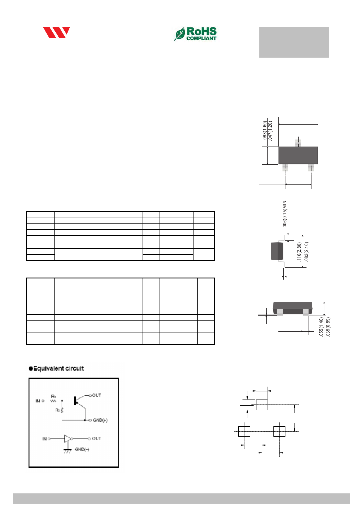
Package outline
SOD-123H
SOT-23
0.146(3.7)
0.130(3.3)
0.012(0.3) Typ.
.122(3.10)
.106(2.70)
0.071(1.8)
0.056(1.4)
.080(2.04)
.070(1.78)
0.040(1.0)
0.024(0.6)
• Case : Molded plastic, SOD-123H
Absolute•
mTearmxiimnaulsm:Prlaatteidntgesrm@ina2l5s,кsolderable
per
,
MIL-STD-750
Symbol
MPeathraomd e2t0e2r 6
Min Typ Max Unit
0.031(0.8) Typ.
0.031(0.8) Typ.
VCC • PSouplaprlyityvo:ltIangdeicated by cathode band ---
50
---
V
VIN
Input voltage
-5
--- +12
V
Pd • MPoowuenrtidnisgsPipoatsioitnion : Any
--- 200 --- mW
Dimensions in inches and (millimeters)
Tj • WJuenicgtihotn:tAempppreoraxtiumreated 0.011 gram --- 150 ---
ć
Tstg
Storage temperature
-55 --- 150
ć
IO
Output McuArreXnItMUM RATINGS AND ELECT1R00ICAL CHARmAA CTERISTICS
IC(MAX)
100
Ratings at 25℃ ambient temperature unless otherwise specified.
ElecSFoitnrrgiclceaappalhcCaitsihveeahrlaoalafcdw,taedvereri,as6tte0iHccuzsr,r@reenst2isb5tyivк2e0o%f inductive load.
Symbol
Parameter
Min Typ Max Unit
.008(0.20)
.003(0.08)
VI(off)
Input voltageR(VACTCI=N5GVS, IO=100A)
VMI(aonr)king Code
(VO=0.3V, IO=5mA)
0S.5YMBOL---FM120-M-H-- FM130-MVH FM140-MH FM150-MH FM160-MH FM180-MH FM1100-MH FM1150-MH FM1200-MH
---
--- 12 1.1 13 V 14
15
16
18
10
115 120
VMOa(oxn)imum OReuctpuurrtevnotlPtaegaek(RIOe=v5emrsAe,IVi=o0lt.a2g5emA)
II
Input current (VI=5V)
IMO(aofxf)imum ROMutSpuVtoclutargreent (VCC=50V, VI=0)
MGaIximum DC BculorcreknintggVaoinlta(VgOe=5V, IO=10mA)
--V- RRM 0.1 20 0.3 30 V 40
50
60
80
100
150
200
---
---
3.6 mA
.004(0.10)MAX.
--V- RMS --- 14 0.5 21A 28
35
42
56
70
105
140
80VDC --- 20 --- 30
40
50
60
80
100
150
200
MRa1ximum AInvpeurtargeesFisotarwnacerd Rectified Current
R2/R1 Resistance ratio
1.54IO 2.2
17 21
PsufeTpaekriFmoprwosaT(eVrrddaOSo=nnus1ri0rtgaiVoeten,CdIfOurl=orera5eqdmnute(AJ8nE,.c3Dfy=mE1Cs0s0miMnegtHlhezoh)da) lf sine-wave ---IFSM 250
2.86 K¡
26
--- MHz
1.0 .020(0.50)
.012(0.30)
30
Typical Thermal Resistance (Note 2)
RΘJA
Dimens4i0ons in inches and (millimeters)
Typical Junction Capacitance (Note 1)
Operating Temperature Range
CJ
TJ
-55 to +125
120
-55 to +150
Storage Temperature Range
*MarkingT:SETG42
S-u6g5gteos+t1e7d5 Solder
Pad Layout
CHARACTERISTICS
Maximum Forward Voltage at 1.0A DC
SYMBOL FM120-MH FM130-MH FM140-MH FM150-MH FM.106301-MH FM180-MH FM1100-MH FM1150-MH FM1200-MH
VF
0.50
0.70 .800
0.85
0.9
0.92
Maximum Average Reverse Current at @T A=25℃
IR
Rated DC Blocking Voltage
@T A=125℃
NOTES:
1- Measured at 1 MHZ and applied reverse voltage of 4.0 VDC.
.035
0.5
.900
10
.079
2.000
inches
mm
2- Thermal Resistance From Junction to Ambient
.037
.950
.037
.950
2012-06
2012-0
WILLAS ELECTRONIC CORP
WILLAS ELECTRONIC CORP.
Share Link: 