CY7C1318BV18(2004) Просмотр технического описания (PDF) - Cypress Semiconductor
Номер в каталоге
Компоненты Описание
производитель
CY7C1318BV18 Datasheet PDF : 24 Pages
| |||
PRELIMINARY
CY7C1316BV18
CY7C1916BV18
CY7C1318BV18
CY7C1320BV18
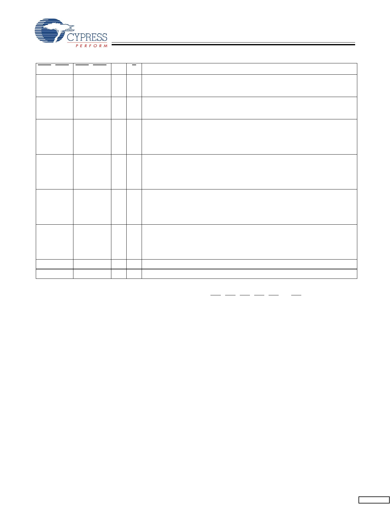
Write Cycle Descriptions (CY7C1316BV18 and CY7C1318BV18)[2, 8]
BWS0,NWS0 BWS1,NWS1 K
K
Comments
L
L
L-H – During the Data portion of a Write sequence:
CY7C1316BV18 − both nibbles (D[7:0]) are written into the device,
CY7C1318BV18 − both bytes (D[17:0]) are written into the device.
L
L
– L-H During the Data portion of a Write sequence:
CY7C1316BV18 − both nibbles (D[7:0]) are written into the device,
CY7C1318BV18 − both bytes (D[17:0]) are written into the device.
L
H
L-H – During the Data portion of a Write sequence:
CY7C1316BV18 − only the lower nibble (D[3:0]) is written into the device. D[7:4]
will remain unaltered,
CY7C1318BV18 − only the lower byte (D[8:0]) is written into the device. D[17:9]
will remain unaltered.
L
H
– L-H During the Data portion of a Write sequence:
CY7C1316BV18 − only the lower nibble (D[3:0]) is written into the device. D[7:4]
will remain unaltered,
CY7C1318BV18 − only the lower byte (D[8:0]) is written into the device. D[17:9]
will remain unaltered.
H
L
L-H – During the Data portion of a Write sequence:
CY7C1316BV18 − only the upper nibble (D[7:4]) is written into the device. D[3:0]
will remain unaltered,
CY7C1318BV18 − only the upper byte (D[17:9]) is written into the device. D[8:0]
will remain unaltered.
H
L
– L-H During the Data portion of a Write sequence:
CY7C1316BV18 − only the upper nibble (D[7:4]) is written into the device. D[3:0]
will remain unaltered,
CY7C1318BV18 − only the upper byte (D[17:9]) is written into the device. D[8:0]
will remain unaltered.
H
H
L-H – No data is written into the devices during this portion of a Write operation.
H
H
– L-H No data is written into the devices during this portion of a Write operation.
Write Cycle Descriptions[2, 8] (CY7C1320BV18)
BWS0 BWS1 BWS2 BWS3 K
L
L
L
L
L-H
K
Comments
– During the Data portion of a Write sequence, all four bytes (D[35:0]) are
written into the device.
L
L
L
L
–
L-H During the Data portion of a Write sequence, all four bytes (D[35:0]) are
written into the device.
L
H
H
H
L-H
– During the Data portion of a Write sequence, only the lower byte (D[8:0]) is
written into the device. D[35:9] will remain unaltered.
L
H
H
H
–
L-H During the Data portion of a Write sequence, only the lower byte (D[8:0]) is
written into the device. D[35:9] will remain unaltered.
H
L
H
H
L-H
– During the Data portion of a Write sequence, only the byte (D[17:9]) is
written into the device. D[8:0] and D[35:18] will remain unaltered.
H
L
H
H
–
L-H During the Data portion of a Write sequence, only the byte (D[17:9]) is
written into the device. D[8:0] and D[35:18] will remain unaltered.
H
H
L
H
L-H
– During the Data portion of a Write sequence, only the byte (D[26:18]) is
written into the device. D[17:0] and D[35:27] will remain unaltered.
H
H
L
H
–
L-H During the Data portion of a Write sequence, only the byte (D[26:18]) is
written into the device. D[17:0] and D[35:27] will remain unaltered.
H
H
H
L
L-H
During the Data portion of a Write sequence, only the byte (D[35:27]) is
written into the device. D[26:0] will remain unaltered.
Note:
8. Assumes a Write cycle was initiated per the Write Port Cycle Description Truth Table. NWS0, NWS1, BWS0, BWS1, BWS2, and BWS3 can be altered on different
portions of a Write cycle, as long as the set-up and hold requirements are achieved.
Document Number: 38-05621 Rev. **
Page 10 of 24
Share Link: 