CY7C1316BV18(2004) Просмотр технического описания (PDF) - Cypress Semiconductor
Номер в каталоге
Компоненты Описание
производитель
CY7C1316BV18 Datasheet PDF : 24 Pages
| |||
PRELIMINARY
CY7C1316BV18
CY7C1916BV18
CY7C1318BV18
CY7C1320BV18
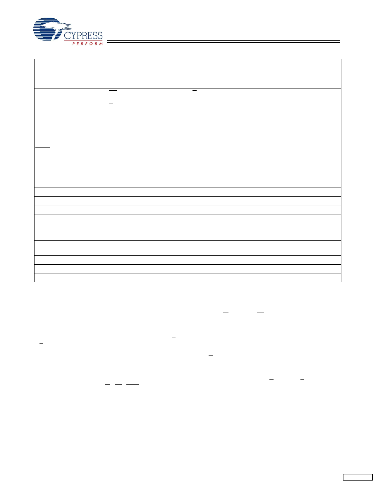
Pin Definitions (continued)
Pin Name
CQ
CQ
ZQ
DOFF
TDO
TCK
TDI
TMS
NC
NC/36M
NC/72M
NC/144M
NC/288M
VREF
VDD
VSS
VDDQ
I/O
Pin Description
Output-
Clock
CQ is referenced with respect to C. This is a free running clock and is synchronized to the
output clock (C) of the DDR-II. In the single clock mode, CQ is generated with respect to K. The
timings for the echo clocks are shown in the AC Timing table.
Output-
Clock
CQ is referenced with respect to C. This is a free running clock and is synchronized to the
output clock (C) of the DDR-II. In the single clock mode, CQ is generated with respect to K. The
timings for the echo clocks are shown in the AC Timing table.
Input
Output Impedance Matching Input. This input is used to tune the device outputs to the system
data bus impedance. CQ, CQ, and Q[x:0] output impedance are set to 0.2 x RQ, where RQ is a
resistor connected between ZQ and ground. Alternately, this pin can be connected directly to VDD,
which enables the minimum impedance mode. This pin cannot be connected directly to GND or
left unconnected.
Input
DLL Turn Off, active LOW. Connecting this pin to ground will turn off the DLL inside the device.
The timings in the DLL turned off operation will be different from those listed in this data sheet.
More details on this operation can be found in the application note, “DLL Operation in the
QDR™-II.”
Output TDO for JTAG.
Input TCK pin for JTAG.
Input TDI pin for JTAG.
Input TMS pin for JTAG.
N/A
Not connected to the die. Can be tied to any voltage level.
N/A
Not connected to the die. Can be tied to any voltage level.
N/A
Not connected to the die. Can be tied to any voltage level.
N/A
Not connected to the die. Can be tied to any voltage level.
N/A
Not connected to the die. Can be tied to any voltage level.
Input- Reference Voltage Input. Static input used to set the reference level for HSTL inputs and Outputs
Reference as well as AC measurement points.
Power Supply Power supply inputs to the core of the device.
Ground Ground for the device.
Power Supply Power supply inputs for the outputs of the device.
Functional Overview
The CY7C1316BV18, CY7C1916BV18, CY7C1318BV18, and
CY7C1320BV18 are synchronous pipelined Burst SRAMs
equipped with a DDR interface.
Accesses are initiated on the rising edge of the positive input
clock (K). All synchronous input timing is referenced from the
rising edge of the input clocks (K and K) and all output timing
is referenced to the rising edge of the output clocks (C/C or
K/K when in single clock mode).
All synchronous data inputs (D[x:0]) pass through input
registers controlled by the rising edge of the input clocks (K
and K). All synchronous data outputs (Q[x:0]) pass through
output registers controlled by the rising edge of the output
clocks (C/C or K/K when in single-clock mode).
All synchronous control (R/W, LD, BWS[0:X]) inputs pass
through input registers controlled by the rising edge of the
input clock (K).
CY7C1318BV18 is described in the following sections. The
same basic descriptions apply to CY7C1316BV18,
CY7C1916BV18, and CY7C1320BV18.
Read Operations
The CY7C1318BV18 is organized internally as a single array
of 1M x 18. Accesses are completed in a burst of two
sequential 18-bit data words. Read operations are initiated by
asserting R/W HIGH and LD LOW at the rising edge of the
positive input clock (K). The address presented to Address
inputs is stored in the Read address register and the least
significant bit of the address is presented to the burst counter.
The burst counter increments the address in a linear fashion.
Following the next K clock rise the corresponding 18-bit word
of data from this address location is driven onto the Q[17:0]
using C as the output timing reference. On the subsequent
rising edge of C the next 18-bit data word from the address
location generated by the burst counter is driven onto the
Q[17:0]. The requested data will be valid 0.45 ns from the rising
edge of the output clock (C or C, or K and K when in single
clock mode, 200-MHz and 250-MHz device). In order to
maintain the internal logic, each read access must be allowed
to complete. Read accesses can be initiated on every rising
edge of the positive input clock (K).
When Read access is deselected, the CY7C1318BV18 will
first complete the pending Read transactions. Synchronous
Document Number: 38-05621 Rev. **
Page 7 of 24
Share Link: 