CXD3068Q Просмотр технического описания (PDF) - Sony Semiconductor
Номер в каталоге
Компоненты Описание
производитель
CXD3068Q Datasheet PDF : 134 Pages
| |||
CXD3068Q
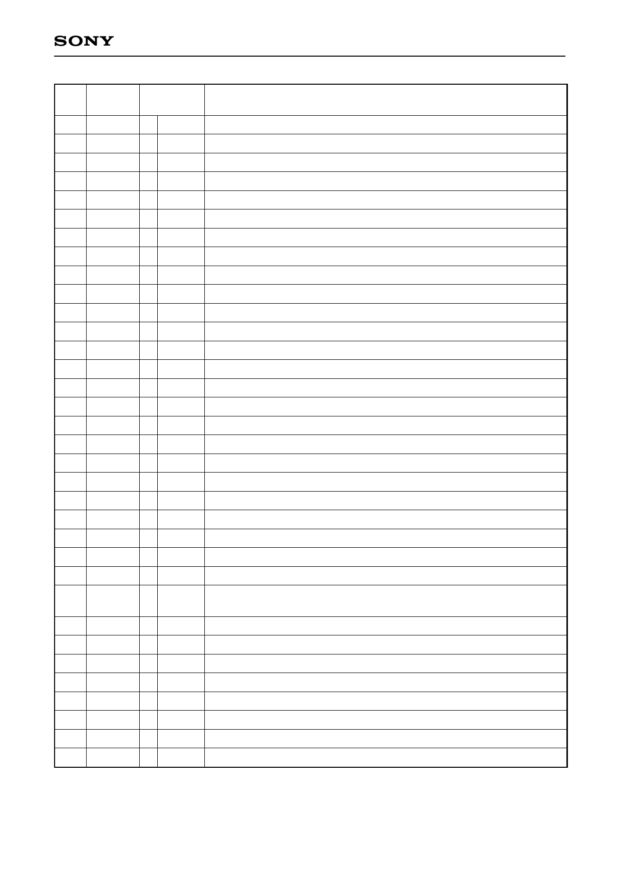
Pin
No.
Symbol
I/O
Description
34 FRDR O 1, 0 Focus drive output.
35 DVSS1 — —
Digital GND.
36 TEST
I
Test. Normally, GND.
37 TES1
I
Test. Normally, GND.
38 VC
I
Center voltage input.
39 FE
I
Focus error signal input.
40 SE
I
Sled error signal input.
41 TE
I
Tracking error signal input.
42 CE
I
Center servo analog input.
43 RFDC I
RF signal input.
44 ADIO
O Analog Test. No connected.
45 AVSS0 — —
Analog GND.
46 IGEN
I
Constant current input for operational amplifier.
47 AVDD0 — —
Analog power supply.
48 ASYO O 1, 0 EFM full-swing output. (low = Vss, high = VDD)
49 ASYI
I
Asymmetry comparator voltage input.
50 RFAC I
EFM signal input.
51 AVSS1 — —
Analog GND.
52 CLTV
I
Multiplier VCO1 control voltage input.
53 FILO
O Analog Master PLL filter output (slave = digital PLL).
54 FILI
I
Master PLL filter input.
55 PCO
O 1, Z, 0 Master PLL charge pump output.
56 AVDD1 — —
Analog power supply.
57 BIAS
I
Asymmetry circuit constant current input.
58 VCTL
I
Wide-band EFM PLL VCO2 control voltage input.
59 V16M
I/O 1, 0
Wide-band EFM PLL VCO2 oscillation output. Serves as wide-band EFM
PLL clock input by switching with the command.
60 VPCO O 1, Z, 0 Wide-band EFM PLL charge pump output.
61 DVDD2 — —
Digital power supply.
62 ASYE
I
Asymmetry circuit on/off (low = off, high = on).
63 MD2
I
Digital Out on/off control (low = off, high = on).
64 DOUT O 1, 0 Digital Out output.
65 LRCK O 1, 0 D/A interface. LR clock output. f = Fs
66 PCMD O 1, 0 D/A interface. Serial data output (two's complement, MSB first).
67 BCK
O 1, 0 D/A interface. Bit clock output.
–5–
Share Link: 