SPX2950ACN-3.3(2003) Просмотр технического описания (PDF) - Signal Processing Technologies
Номер в каталоге
Компоненты Описание
производитель
SPX2950ACN-3.3 Datasheet PDF : 13 Pages
| |||
PROGRAMMING THE OUTPUT
VOLTAGE OF SPX2951
The SPX2951 may be pin-strapped for 5V using
its internal voltage divider by tying Pin 1 (out-
put) to Pin 2 (sense) and Pin 7 (feedback) to Pin
6 (5V Tap). Also, it may be programmed for any
output voltage between its 1.235V reference
and its 30V maximum rating . As seen in Figure
2, an external pair of resistors is required. Refer
to the below equation for the programming of
the output voltage:
VOUT = VREF × (1 + R1/R2)+ IFBR1
The VREF is 1.235 and IFB is the feedback bias
current, nominally -20nA. The minimum rec-
ommended load current of 1 µA forces an upper
limit of 1.2MΩ on value of R2. If no load is
presented the IFB produces an error of typically
2% in VOUT which may be eliminated at room
temperature by trimming R1. To improve the
accuracy choose the value of R2 = 100k this
reduces the error by 0.17% and increases the
resistor program current by 12µA. Since the
SPX2951 typically draws 60µA at no load with
Pin 2 open-circuited this is a small price to pay.
REDUCING OUTPUT NOISE
It may be an advantage to reduce the AC noise
present at the output. One way is to reduce the
regulator bandwidth by increasing the size of
the output capacitor. This is the only way that
noise can be reduced on the 3 lead SPX2950 but
is relatively inefficient, as increasing the ca-
pacitor from 1µF to 220µF only decreases the
noise from 430µV to 160µVRMS for a 100kHz
bandwidth at 5V output. Noise could also be
reduced fourfold by a bypass capacitor across
R1, since it reduces the high frequency gain from
4 to unity. Pick
CBYPASS ≅ (1 / 2πR1 × 200 Hz)
or choose 0.01µF. When doing this, the output
capacitor must be increased to 3.3µF to main-
tain stability. These changes reduce the output
noise from 430µV to 100µVRMS for a 100kHz
bandwidth at 5V output. With the bypass ca-
pacitor added, noise no longer scales with out-
put voltage so that improvements are more dra-
matic at higher output voltages.
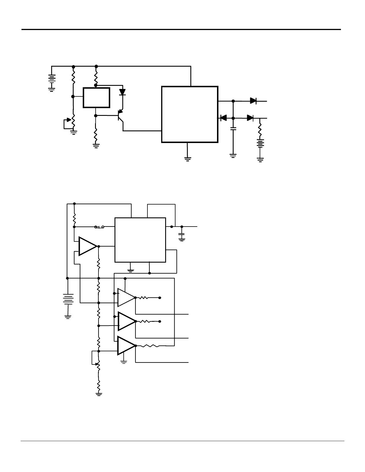
TYPICAL APPLICATIONS
+V IN
100K
ERROR
OUTPUT
8
5 ______ +VIN
ERROR
1
V OUT
SPX2951
SHUTDOWN
INPUT
3
SD
GND
4
FB
7
1.23V
1.2 to 30V
+
R1
3.3µF
.01µF
VREF
R2
Figure 2. Adjustable Regulator
Rev. 3/6/03
SPX2950/SPX2951 150mA Low Dropout Voltage Regulator
9
©Copyright 2003 Sipex Corporation
Share Link: 