AV2188 Просмотр технического описания (PDF) - Unspecified
Номер в каталоге
Компоненты Описание
производитель
AV2188 Datasheet PDF : 20 Pages
| |||
AV2188
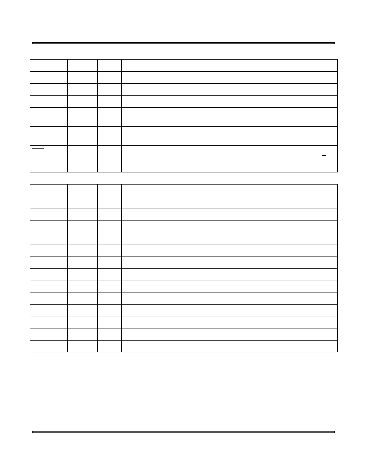
PIN DESCRIPTION (Continued)
Pin Name
DVSS
XCK
SCL
SDA
TEST
RST
Analog
VOL3
VOR3
VOL2
VOR2
VOL1
VOR1
AVSS
VCM2
AVDD
VCM1
AVSS
AINR
AINL
N/C
Pin #
9
10
11
12
11
12
28
27
26
25
24
23
22
21
20
19
18
17
16
15
Type
Description
GND Digital ground
I External Master Clock Input.
I I2C clock input.
I/O I2C DATA bus. Open drain ouput. Externally this pin should tie to a 680 ohm pull
up resistor.
O Test fs reference pin. For test vector verification. For normal operation this pin
must be tied to ‘0’.
I Active low power down reset. When low, the chip is reset and all programmable
registers are reset to default values. Must activate this pin if the P/S or
ADDR[1:0] change state.
O Analog left channel output 3
O Analog right channel output 3.
O Analog left channel output 2.
O Analog right channel output 2.
O Analog left channel output 1.
O Analog right channel output 1.
GND Analog circuits ground
Common voltage output pin for the DAC.
+5V Analog circuits power supply
Common voltage output pin for the ADC.
GND Analog circuits ground
I ADC right cahnnel input. 1 volt rms input.
I ADC left channel input. 1 volt rms input.
No connection, should be tied to AVSS
5-20
June 2, 2000
Share Link: 