AM27X010 Просмотр технического описания (PDF) - Advanced Micro Devices
Номер в каталоге
Компоненты Описание
производитель
AM27X010 Datasheet PDF : 10 Pages
| |||
AC CHARACTERISTICS
Parameter Symbols
Am27X010
JEDEC Standard
Description
Test Setup -55 -70 -90 -120 -150 -200 -255 Unit
tAVQV
tACC Address to Output Delay
CE#,
OE# = VIL
Max
55
70
90 120 150 200 250 ns
tELQV
tCE
Chip Enable to Output Delay OE# = VIL Max 55 70 90 120 150 200 250 ns
tGLQV
tOE
Output Enable to Output Delay CE# = VIL Max 35 35 40 50 65 75 75 ns
tEHQZ
tGHQZ
tDF
(Note 2)
Chip Enable High or Output
Enable High to Output High Z,
Whichever Occurs First
Max 25 25 25 35 35 40 40 ns
tAXQX
Output Hold Time from
tOH
Addresses, CE# or OE#,
Whichever Occurs First
Min 0 0 0 0 0 0 0 ns
Caution: Do not remove the device from (or insert it into) a socket or board that has VPP or VCC applied.
Notes:
1. VCC must be applied simultaneously or before VPP, and removed simultaneously or after VPP.
2. This parameter is sampled and not 100% tested.
3. Switching characteristics are over operating range, unless otherwise specified.
4. See Figure 3 and Table 1 for test specifications.
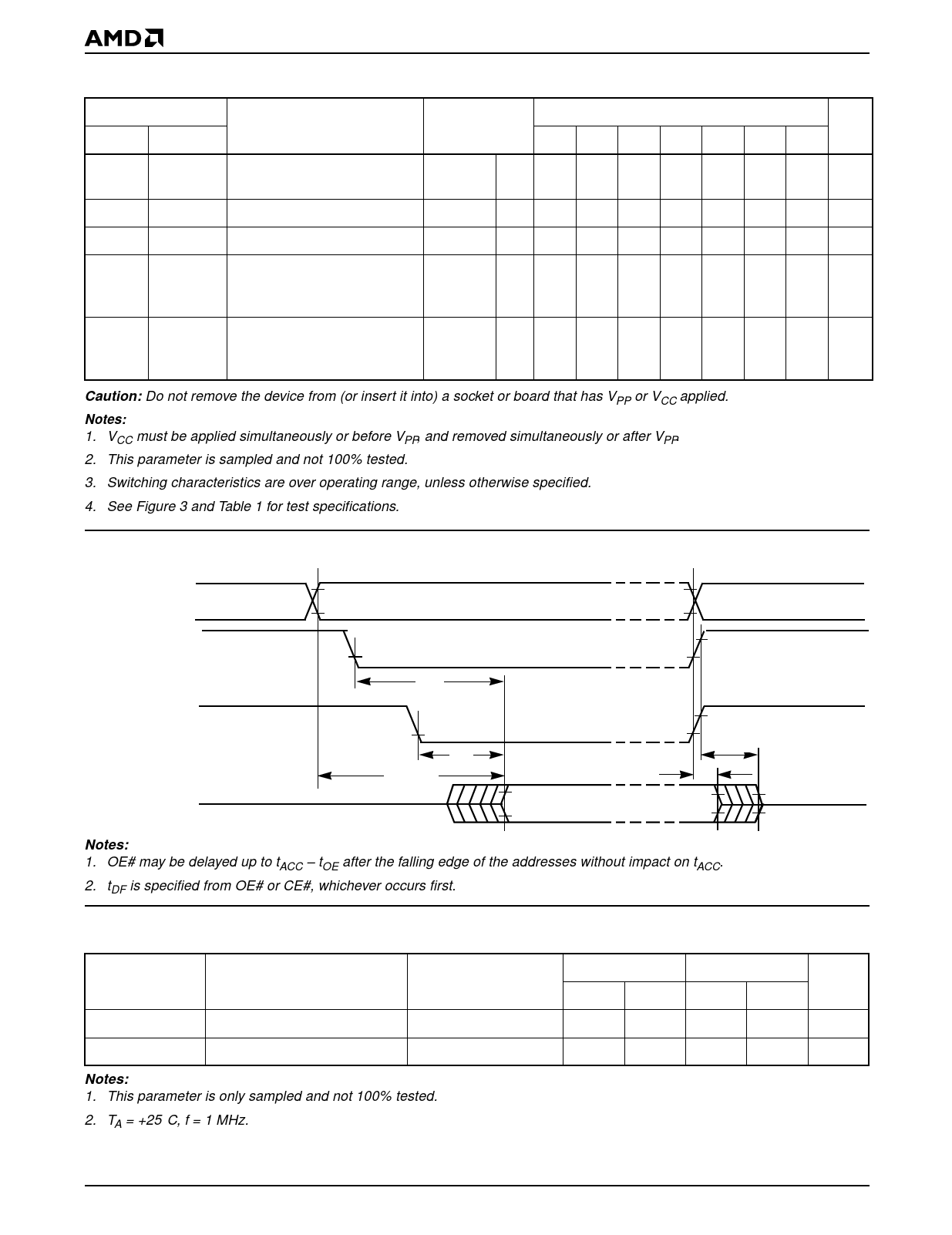
SWITCHING WAVEFORMS
2.4
Addresses
0.45
2.0
0.8
Addresses Valid
2.0
0.8
CE#
tCE
OE#
Output
High Z
tOE
tACC
(Note 1)
tOH
Valid Output
tDF (Note 2)
High Z
12080F-9
Notes:
1. OE# may be delayed up to tACC – tOE after the falling edge of the addresses without impact on tACC.
2. tDF is specified from OE# or CE#, whichever occurs first.
PACKAGE CAPACITANCE
Parameter
Symbol
Parameter Description Test Conditions
CIN
Input Capacitance
VIN = 0
COUT
Output Capacitance
VOUT = 0
Notes:
1. This parameter is only sampled and not 100% tested.
2. TA = +25°C, f = 1 MHz.
PD 032
PL 032
Typ
Max
Typ
Max
Unit
8
12
8
10
pF
11
14
11
12
pF
8
Am27X010
Share Link: 