7805ALPRPDH Просмотр технического описания (PDF) - MAXWELL TECHNOLOGIES
Номер в каталоге
Компоненты Описание
производитель
7805ALPRPDH Datasheet PDF : 18 Pages
| |||
16-Bit Latchup Protected ADC
7805ALP
In order to prevent backdriving the supply, the STATUS signal should be used in the system to tri-state or gate external
I/O drive circuits to a low state. Similarly, if the data outputs are connected to a bus with other bus driver circuits, all
external data bus drivers must be tri-stated and individual pull up resistors to the supply voltage (if used on the data
bus) must not be less than 10 KΩ typical to assure proper single event effect recovery. Tri-stating of inputs should
occur within 100 nsec after the rise of the status pin. The BYTE signal can be made available in place of the STATUS
signal at customer request.
STATUS can also be used to generate an input to the system data processor indicating that an LPT™ cycle has
occurred, and the protected device output accuracy may not be met until after the respective recovery time to the
event. The STATUS signal is generated from an advanced CMOS logic gate output. This output may not exhibit a
monotonic falltime and may even oscillate briefly while power is being restored to the protected device and the decou-
pling capacitance is charged. Loading on the STATUS output should be minimized because this signal is used inter-
nally by the 7805A. It is recommended that load current not exceed 2 mA and load capacitance be kept well below
1000 pF.
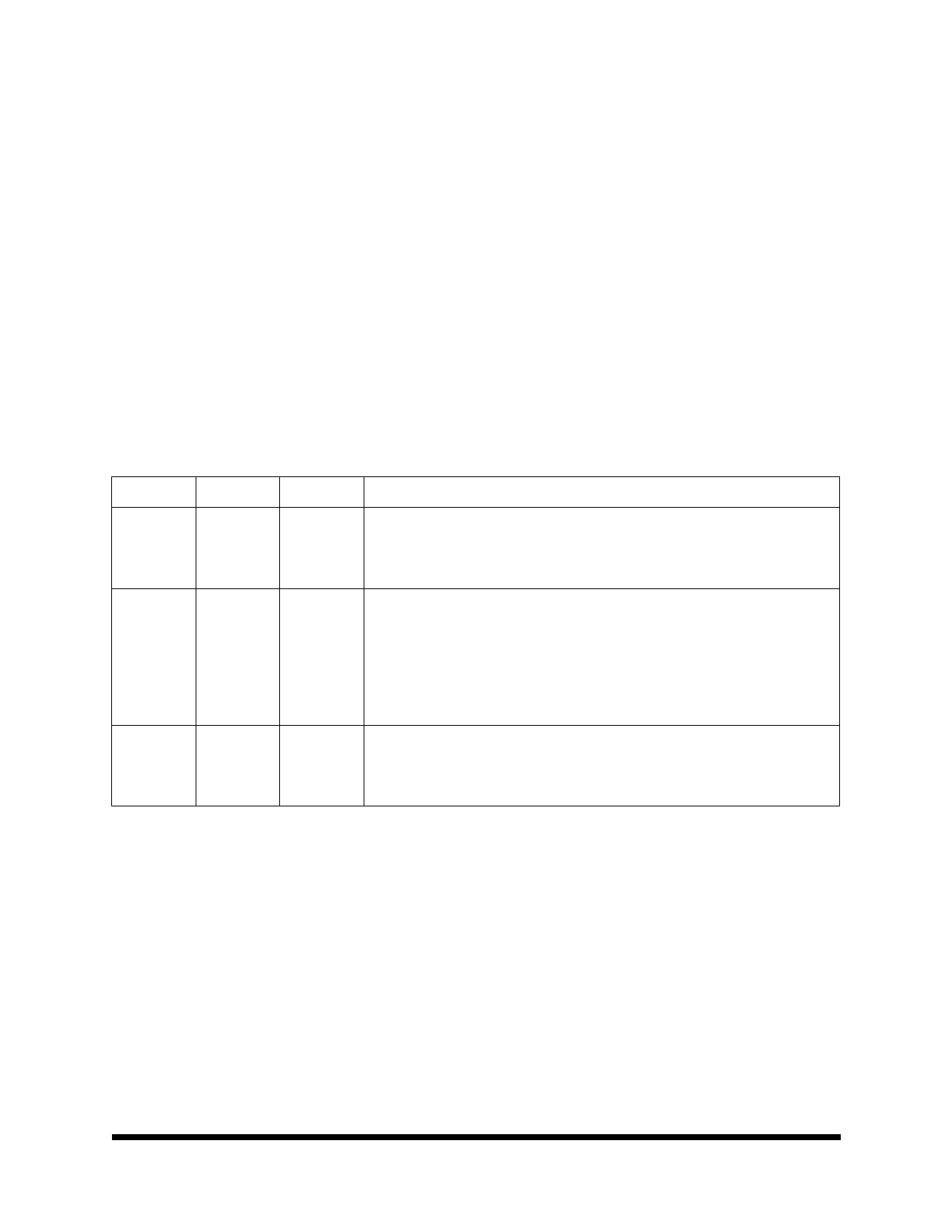
A summary of the pin differences between the ADS7805 and 7805A is provided below.
PIN NUMBER
23
27
28
ADS7805
BYTE
VANA
VDIG
TABLE 16. PIN DIFFERENCES
7805A PIN DIFFERENCE DESCRIPTION
STATUS
DECPLNG
VS
A high level STATUS signal indicates that power is removed from the ADS7805 die.
I/O pins must not be driven high while this signal is active. The BYTE signal of the
ADS7805 die is internally grounded but can also be made available in place of the
STATUS pin at customer request.
The ADS7805 VANA and VDIG die pads are connected together and are available
at the DECPLNG pin. This pin allows external ceramic capacitors to directly decou-
ple the power inputs to the ADS7805 die-to-analog ground. Decoupling capaci-
tance should not exceed 0.2 uF typical. This pin must not be connected to a power
supply directly since this will defeat the latchup protection circuitry. Electrolytic filter
capacitors should not be connected to this pin but should be connected between
the VS pin and ground.
This is the power supply input for the LPT circuitry and the protected ADS7805 die.
This supply should be treated as an analog supply with filtering and/or isolation
from the noisy system digital power supply. The LPT latchup current sense and
power switch circuitry is located between this pin and the DECPLNG pin.
Example Circuits for Using the 7805A
Figure 2 shows a typical application circuit for using the 7805A as an input to a digital data processor. This circuit
shows the use of the STATUS pin to tri-state the control inputs when the latchup protection circuit cycles the power to
the protected ADS7805 die.
Figure 3 shows a typical application circuit for connecting the 7805A to a 16-bit data bus with multiple drivers on the
bus. Tri-state buffers are used to isolate the 7805A data outputs from the data bus. Figure 4 shows the typical applica-
tion circuit for connecting the 7805A to an 8-bit data bus.
01.10.05 Rev 9
All data sheets are subject to change without notice 10
©2005 Maxwell Technologies
All rights reserved.
Share Link: 