1318 –Я—А–Њ—Б–Љ–Њ—В—А —В–µ—Е–љ–Є—З–µ—Б–Ї–Њ–≥–Њ –Њ–њ–Є—Б–∞–љ–Є—П (PDF) - Linear Technology
–Э–Њ–Љ–µ—А –≤ –Ї–∞—В–∞–ї–Њ–≥–µ
–Ъ–Њ–Љ–њ–Њ–љ–µ–љ—В—Л –Ю–њ–Є—Б–∞–љ–Є–µ
–њ—А–Њ–Є–Ј–≤–Њ–і–Є—В–µ–ї—М
1318 Datasheet PDF : 8 Pages
| |||
LTC1318
PIN FUNCTIONS
C2+, C2вАУ (Pins 22, 23): C2 inputs. Connect a 0.1¬µF capacitor
between C2+ and C2вАУ.
VвАУ (Pin 24): Charge Pump Negative Output. This pin
requires a 0.1µF capacitor to ground. Under normal opera-
tion, this pin maintains a voltage of about 8.6V below
ground. An external load can be connected between this
pin and ground or V+.
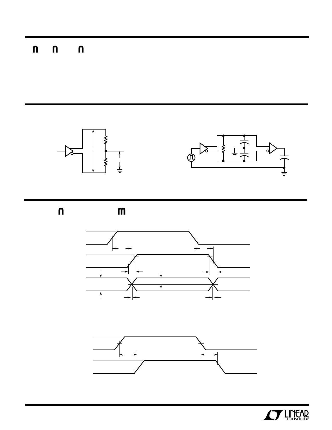
TEST CIRCUITS
+
RL/2
TXD+
TXD
VOD
TXDвАУ
+
RL/2 VOC
вАУ
вАУ
1318 F01
Figure 1.
U
W
SWITCHING WAVEFORMS
TXD
TXD+
RD
TXDвАУ
CL RXD+
CL
RXDвАУ/
RXI2
RXD0/RXD2
CL
Figure 2.
1318 F02
3V
TXD
0V
VO
вАУVO
TXDвАУ
TXD+
f = 1MHz: tr вЙ§ 10ns: tf вЙ§ 10ns
1.5V
1.5V
tPLH
50%
10%
tr
90% VDIFF = V(TXD+) вАУ V(TXDвАУ )
1/2 VO
tPHL
90%
50%
10%
tf
VO
tSKEW
tSKEW
LT1318 вАҐ F03
Figure 3. Differential Driver
V OD2
(RXD+) вАУ (RXDвАУ)
вАУVOD2
VOH
RXDO
VOL
f = 1MHz: tr вЙ§ 10ns: tf вЙ§ 10ns
tPLH
1.5V
tPHL
1.5V
Figure 4. Differential Receiver
LT1318 вАҐ F04
6
Share Link: 