VV5402 Просмотр технического описания (PDF) - Vision
Номер в каталоге
Компоненты Описание
производитель
VV5402 Datasheet PDF : 16 Pages
| |||
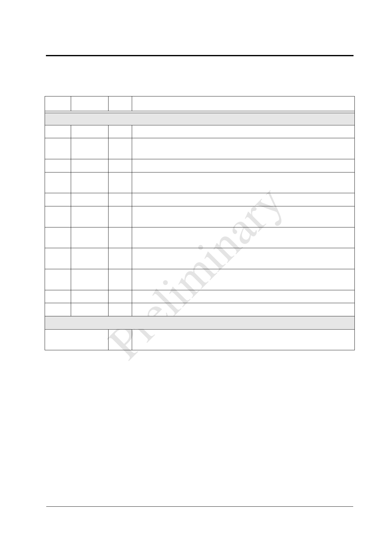
Pin List
Pin
Name Type
Description
DIGITAL CONTROL SIGNALS
16
SAB1
ID↓ Chip Address, Bit 1
17
SIN
ID↓ Used to reset video timing control logic without resetting any other part of
VV5402. Resets video logic on the falling edge of the SIN pulse.
18
SCE
ID↓ Scan Mode Enable - only relevant to test mode.
19
LIN
ID↓ Gamma corrected or Linear output. LIN = 0, gamma corrected output,
LIN = 1, linear output. Default is gamma.
20
SAB0
ID↓ Chip Address, Bit 0
21
AEC
ID↑ Automatic exposure control. AEC = 1, auto exposure is enabled; AEC = 0
auto exposure and auto gain control are disabled.
22
AGC
ID↑ Automatic gain control enable. AGC = 1, auto-gain is enabled (if AEC = 1);
AGC = 0, auto-gain is disabled.
23
CCIR
ID↑ Select default video mode for power-on. CCIR = 1 for CCIR video. EIA
video mode is selected when CCIR = 0. Default is CCIR if unconnected
28
BKLIT
ID↓ Normal or Backlit exposure control mode. BKLIT = 0, normal mode; BKLIT
= 1, backlit mode. Default is normal. See Exposure Control for details.
29
RESETB ID↑ Active low camera reset. All camera systems are reset to power-on state.
38
SCI
ID↓ Scan Chain Input - only relevant to test mode.
OTHER PINS
6, 11, 12, 30, 32,
33, 35, 36, 39, 40
DNC DO NOT CONNECT. These pins must be left ‘floating’ for correct opera-
tion.
Key:
OA -
OD -
OD↓ -
BI -
Analogue output
Digital output
Digital output with internal pull-down
Bidirectional
IA -
ID -
ID↑ -
DNC-
Analogue input
Digital input
Digital input with internal pull-up
Do Not Connect
09/04/97
11
Share Link: 